PCB بهعنوان حامل بسیاری از قطعات و بهعنوان مرکز انتقال سیگنال مدار عمل میکند. این برد به یکی از بخشهای بسیار مهم و کلیدی در محصولات اطلاعاتی الکترونیکی تبدیل شده است. سطح کیفیت و قابلیت اطمینان PCB کیفیت و قابلیت اطمینان کل دستگاه را تعیین میکند.
با کوچکسازی محصولات اطلاعاتی الکترونیکی و فشار برای مقررات زیستمحیطی بدون سرب و بدون هالوژن، بردهای مدار چاپی به سمت چگالی بالاتر، دمای انتقال بالاتر (Tg) و مواد سازگارتر با محیطزیست حرکت کردهاند. اما بهدلیل محدودیتهای هزینه و فناوری، بسیاری از خرابیها در طول تولید PCB و استفاده. این خرابیها باعث بروز اختلافات زیادی در کیفیت میشوند. برای یافتن علت وقوع خرابیها، یافتن راههایی برای رفع آنها و تعیین مسئولیت، لازم است تحلیل خرابیهایی که رخ میدهند انجام شود.
مراحل پایهای در تحلیل خرابی
برای تعیین دقیق علت یا مکانیزم خرابی یا نقص برد مدار چاپی (PCB)، باید اصول اساسی و جریان تحلیل را دنبال کرد. اگر این اصول را رعایت نکنید، ممکن است اطلاعات ارزشمند مربوط به خرابی را از دست بدهید. تحلیل ممکن است متوقف شود یا نتیجهای نادرست بدهد. یک جریان پایهٔ رایج به شرح زیر است.
ابتدا، بر اساس علامت خرابی، اطلاعات جمعآوری کنید، تستهای عملکردی، تستهای الکتریکی و بازرسیهای بصری ساده را انجام دهید. از این اطلاعات برای یافتن ناحیه معیوب و نوع خرابی استفاده کنید. این عمل مکانیابی خرابی یا عیبیابی است.
برای PCBهای ساده یا ساده برد مدار چاپی مونتاژشده در بردها، یافتن بخش معیوب آسان است. اما برای دستگاهها یا زیرلایههای پیچیده، مانند BGA در بستههای MCM، نواقص بهراحتی با میکروسکوپ دیده نمیشوند. در ابتدا یافتن آنها دشوار است. در آن زمان به روشهای دیگری نیاز است.
سپس مکانیزم خرابی را تحلیل کنید. از روشهای فیزیکی و شیمیایی برای بررسی مکانیزمی که منجر به خرابی یا نقص برد مدار چاپی (PCB) شده است، استفاده کنید. این مکانیزمها ممکن است شامل لحیمکاری سرد، آلودگی، آسیب مکانیکی، تنش ناشی از رطوبت، خوردگی دیالکتریک، آسیب ناشی از خستگی، مهاجرت CAF یا یونی، بارگذاری بیش از حد تنش و غیره باشند.
پس از آن، علت اصلی خرابی را تحلیل کنید. بر اساس مکانیزم خرابی و فرآیند تولید، به دنبال دلایلی باشید که باعث وقوع این مکانیزم شدهاند. در صورت نیاز، برای تأیید علت آزمایش انجام دهید. هر زمان که ممکن باشد باید آزمونهای اعتبارسنجی را اجرا کنید. آزمایشها میتوانند علت دقیق وقوع خرابی را مشخص کنند.
این امر پایهای روشن و هدفمند برای گام بعدی بهبود فراهم میکند. گزارش تحلیل شکست را بر اساس دادههای آزمون، حقایق و نتایج تحلیل تهیه کنید. حقایق باید واضح باشند. استدلال باید محکم باشد. چیدمان باید منظم باشد. بدون مدرک، علتی را فرض نکنید.
در حین تحلیل، از روشهای ساده تا پیچیده، از بیرون به درون و از غیرمخرب به مخرب استفاده کنید. این قواعد پایه را دنبال کنید. تنها با این کار میتوانید از دست دادن اطلاعات کلیدی و ایجاد مکانیزمهای شکست جدید ناشی از دخالت انسان جلوگیری کنید.
این مثل یک تصادف رانندگی است. اگر یکی از طرفین صحنه را تخریب کند یا فرار کند، حتی یک افسر پلیس ماهر هم نمیتواند در مورد مسئولیت قضاوت درستی داشته باشد. قانون راهنمایی و رانندگی معمولاً طرفی را که فرار کرده یا صحنه را تخریب کرده است، ملزم به پذیرش تمام مسئولیت میکند.
همین موضوع در مورد تحلیل خرابی PCB یا PCBA نیز صادق است. اگر کسی از هویه برای اصلاح یک اتصال لحیم معیوب استفاده کند یا با قیچی سنگین PCB را قطع کند، تحلیل بعدی غیرممکن میشود. صحنه خرابی از بین میرود. این امر بهویژه زمانی بد است که تنها چند نمونه معیوب وجود داشته باشد. اگر صحنه خرابی آسیب ببیند، علت واقعی قابل شناسایی نخواهد بود.
تکنیکهای تحلیل خرابی
میکروسکوپ نوری
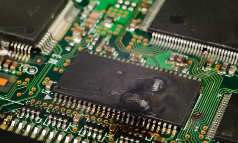
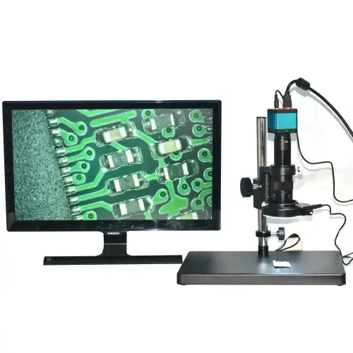
میکروسکوپ نوری عمدتاً برای بازرسی چشمی PCB بهکار میرود. از آن برای یافتن ناحیه معیوب و شواهد فیزیکی مرتبط استفاده کنید. این روش قضاوت اولیهای درباره نوع خرابی ارائه میدهد. بازرسی چشمی به دنبال آلودگی PCB، خوردگی، ترکخوردگی بردها، ردهای مدار و الگوهای خرابی است. برای مثال، بررسی کنید که آیا خرابیها بهصورت دستهای رخ میدهند یا موارد جداگانهاند. بررسی کنید که آیا خرابیها همیشه در یک ناحیه متمرکز میشوند یا خیر.
اشعه ایکس (بازرسی با اشعه ایکس)
برای قطعاتی که با بازرسی چشمی قابل مشاهده نیستند، یا برای عیوب داخلی در سوراخهای عبوری و سایر نواقص درونی، از سیستم تصویربرداری اشعه ایکس استفاده کنید. سیستم اشعه ایکس با جذب یا عبور متفاوت اشعه ایکس توسط مواد با ضخامت یا چگالی مختلف کار میکند. این امر تصاویر را ایجاد میکند. افراد اغلب از اشعه ایکس برای بازرسی عیوب داخلی در اتصالات لحیمشده PCB (برد مدار چاپی)، عیوب داخلی در سوراخهای عبوری و یافتن اتصالات لحیم معیوب در بستهبندیهای با چگالی بالا مانند BGA یا CSP استفاده میکنند.
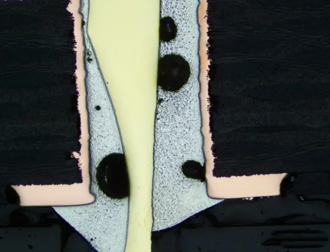
تحلیل مقطع عرضی
تحلیل مقطع عرضی به معنای نمونهبرداری، جاسازی، برش، صیقلکاری، حکاکی و مشاهده مقطع عرضی برد مدار چاپی است. این فرایند ساختار داخلی برد مدار چاپی را نشان میدهد. از طریق تحلیل مقطع عرضی، اطلاعات غنی ریزمورفولوژیکی درباره ویژگیهای برد مدار چاپی (مانند سوراخهای عبوری و آبکاری) به دست میآید. این امر به هدایت بهبودهای کیفی کمک میکند. اما این روش مخرب است. به محض برش نمونه، آن نابود میشود.
میکروسکوپی آکوستیک اسکنی (SAM)
امروزه، ابزار اصلی برای تحلیل بستهبندی و مونتاژ، میکروسکوپ صوتی اسکنی حالت-C است. این روش از امواج فراصوت با فرکانس بالا استفاده میکند. این امواج در ناهمسانیهای ماده بازتاب مییابند. تغییر در دامنه، فاز و قطبیت برای تشکیل تصاویر بهکار میرود. اسکن در امتداد محور Z حرکت میکند تا اطلاعات صفحه X-Y را ثبت کند.
بنابراین، SAM میتواند بسیاری از نقصهای داخلی در قطعات، مواد و PCBها یا PCBAs را تشخیص دهد. این روش ترکها، جداشدگی لایهها، ناخالصیها و حفرهها را شناسایی میکند. اگر محدوده فرکانسی SAM به اندازه کافی وسیع باشد، میتواند نقصهای داخلی در اتصالات لحیم را نیز تشخیص دهد.
تصاویر معمول SAM از رنگ هشداردهنده مانند قرمز برای نشان دادن نواقص استفاده میکنند. در جریان انتقال از فرآیندهای SMT سربدار به بدون سرب، مشکلات زیادی مرتبط با رطوبت در فرآیند ریفلو بروز کرده است. بستهبندیهای پلاستیکی که رطوبت جذب کردهاند، هنگام ریفلو شدن در دماهای بالاتر فرآیندهای بدون سرب ممکن است لایهلایه شده یا از داخل ترک بخورند. بردهای مدار چاپی معمولی نیز در این دماهای بالاتر ممکن است ترک بخورند یا لایهلایه شوند.
در این مورد، SAM مزایای ویژهای برای آزمون غیرمخرب بردهای چندلایه با چیدمان متراکم PCB ارائه میدهد. با این حال، ترکهای بزرگ قابل رؤیت یا بردهای سوخته معمولاً با بازرسی بصری ساده قابل تشخیص هستند.
میکرو-FTIR (تحلیل فروسرخ در مقیاس میکرو)
تحلیل میکرو-فراسرخ، طیفسنجی فروسرخ را با میکروسکوپ ترکیب میکند. این روش از این واقعیت بهره میبرد که مواد مختلف—عمدتاً مواد آلی—نور فروسرخ را بهطور متفاوتی جذب میکنند. بدین ترتیب میتوان اجزای شیمیایی یک ماده را تحلیل کرد. با استفاده از میکروسکوپ، نور مرئی و فروسرخ میتوانند از یک مسیر نوری مشترک عبور کنند. در میدان دید مرئی میتوان مقادیر اندکی آلودگی آلی را برای تحلیل یافت.
بدون میکروسکوپ، طیفسنجی فروسرخ معمولاً به مقدار نمونهٔ بیشتری نیاز دارد. در فرایندهای الکترونیکی، آلودگیهای بسیار کوچک میتوانند باعث کاهش کیفیت لحیمپذیری پد یا پایه شوند. بنابراین بدون طیفسنجی فروسرخ متصل به میکروسکوپ، حل برخی مشکلات فرآیند دشوار است. میکرو-FTIR عمدتاً برای تحلیل آلودگیهای آلی روی سطوح لحیم یا در اتصالات لحیم و همچنین برای بررسی علل خوردگی یا کاهش کیفیت لحیمپذیری استفاده میشود.
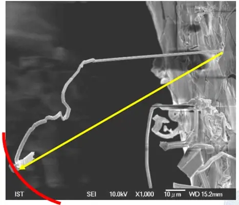
میکروسکوپ الکترونی روبشی (SEM)
میکروسکوپ الکترونی روبشی یک سامانهٔ بزرگ تصویربرداری مفید برای تحلیل خرابی است. از آن برای مشاهدهٔ ریختشناسی استفاده میشود. میکروسکوپهای الکترونی روبشی مدرن قدرتمند هستند. آنها میتوانند ساختارهای ریز یا ویژگیهای سطحی را تا صدها هزار برابر بزرگنمایی کنند.
در تحلیل خرابی برد مدار چاپی یا محل اتصال لحیم، میکروسکوپ الکترونی روبشی (SEM) عمدتاً برای بررسی سازوکارهای خرابی بهکار میرود. بهطور مشخص، SEM برای مشاهده ریختشناسی سطحی پدها، ساختار متالوگرافی محلهای اتصال لحیم، اندازهگیری ترکیبات بینفلزی، تحلیل پوششهای قابل لحیم و تحلیل و اندازهگیری ویسکرهای قلع استفاده میشود.
در مقایسه با میکروسکوپ نوری، میکروسکوپ الکترونی روبشی (SEM) تصویر الکترونی ایجاد میکند، بنابراین سیاه و سفید است. نمونههای SEM باید رسانا باشند. برای غیررساناها و برخی نیمهرساناها باید نمونه را با طلا یا کربن پوشش دهید. در غیر این صورت، بار الکتریکی روی سطح نمونه تجمع یافته و بر مشاهده تأثیر میگذارد. تصاویر SEM عمق میدان بسیار بیشتری نسبت به میکروسکوپهای نوری دارند. برای ساختارهای متالورژیکی، سطوح ریزترک و ویسکرهای قلع، SEM یک روش تحلیلی مهم است.
تحلیل حرارتی
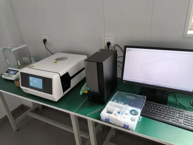
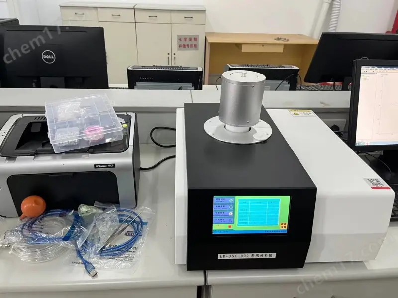
کالریمتری تفاضلی اسکنی (DSC)
DSC اختلاف توان بین نمونهٔ آزمایشی و مرجع را تحت کنترل دما توسط برنامه اندازهگیری میکند. این دستگاه رابطه بین اختلاف توان و دما یا زمان را ثبت میکند. DSC بررسی میکند که گرما چگونه با دما تغییر میکند. بر اساس آن میتوانید رفتار فیزیکی، شیمیایی و ترمودینامیکی مواد را مطالعه کنید.
DSC کاربردهای زیادی دارد. در تحلیل PCB، DSC عمدتاً برای اندازهگیری درجهٔ پخت و دمای انتقال شیشهای (Tg) پلیمرهای بهکاررفته در PCB استفاده میشود. این دو پارامتر قابلیت اطمینان PCB را در مراحل بعدی فرآیند تعیین میکنند.
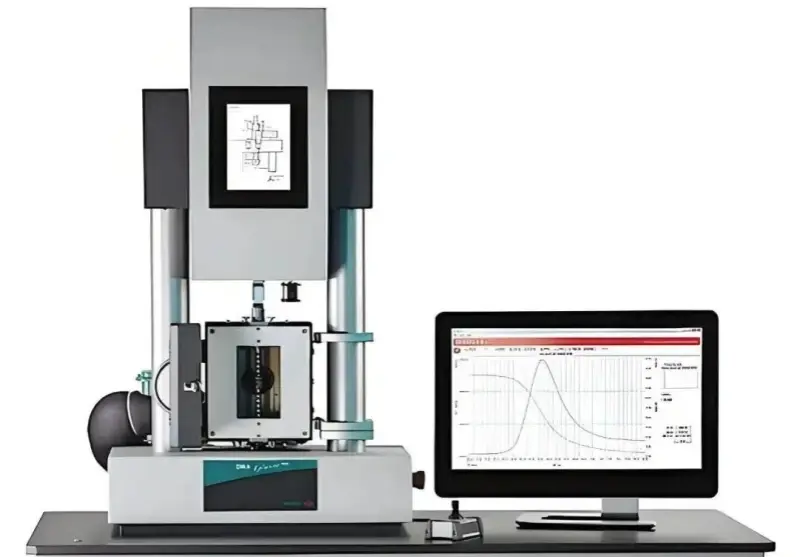
تحلیل ترمومکانیکی (TMA)
TMA رفتار تغییرشکل جامدات، مایعات و ژلها را تحت کنترل دما یا نیروی مکانیکی برنامهریزیشده اندازهگیری میکند. این روش پیوند بین رفتار حرارتی و مکانیکی را بررسی میکند. با مطالعه تغییرشکل در مقابل دما (یا زمان)، میتوان خواص فیزیکی و شیمیایی ماده و ترمودینامیک آن را بررسی کرد.
در تحلیل PCB، TMA عمدتاً دو پارامتر کلیدی را اندازهگیری میکند: ضریب انبساط خطی و دمای انتقال شیشهای. اگر ماده پایه ضریب انبساط بالایی داشته باشد، PCB اغلب پس از لحیمکاری و مونتاژ دچار شکستگی ویای فلزیشده میشود.
آنالیز ترموگراویمетریک (TGA)
TGA تغییر جرم یک ماده را تحت کنترل دما یا زمان برنامهریزیشده اندازهگیری میکند. با ترازویی دقیق، TGA میتواند تغییرات جزئی جرم را در طول اجرای آزمایش در دمای کنترلشده ردیابی کند.
از منحنی تغییر جرم در مقابل دما (یا زمان)، میتوانید رفتار فیزیکی و شیمیایی ماده و ترمودینامیک آن را مطالعه کنید. در تحلیل PCB، TGA عمدتاً برای اندازهگیری پایداری حرارتی یا دمای تجزیه مواد PCB استفاده میشود. اگر زیرلایه دمایی بسیار پایین برای تجزیه داشته باشد، PCB در حین لحیمکاری در دمای بالا جدا یا ترکخوردگی خواهد داشت.
نکات پایانی و یادآوریهای بهترین شیوهها
هنگام برنامهریزی تحلیل شکست، از رویکردی روشن و گامبهگام پیروی کنید. با بازرسیهای بصری و غیرمخرب آغاز کنید. از آزمونهای الکتریکی و جمعآوری اطلاعات استفاده کنید. سپس به روشهای تصویربرداری مانند اشعه ایکس و SAM روی آورید. در صورت نیاز، از ابزارهای ریزوشیمیایی مانند ریز-FTIR و تصویربرداری سطحی مانند SEM بهره ببرید. آزمونهای مخرب مانند برش عرضی را برای زمانی که به اطلاعات ریزساخت نیاز دارید و مقدار نمونه اجازه تخریب را میدهد، در نظر بگیرید.
همیشه دادهها را ثبت کنید و حقایق را واضح نگه دارید. از سادهترین مراحل منطقی استفاده کنید. در صورت امکان نتایج را با آزمایشها اثبات کنید. قبل از مستندسازی صحنهٔ خرابی، آن را تغییر یا آسیب ندهید، زیرا با تغییر صحنه، علت واقعی ممکن است از بین برود. از این قاعده پیروی کنید: از ساده به پیچیده، از بیرون به داخل، از غیرخرابیزا به خرابیزا. این کار در زمان صرفهجویی میکند و نتایج تحلیل را صحیح ارائه میدهد.