Materials, Types &
Applications for
Harsh Environments
Engineered to endure extreme temperatures, high humidity, constant vibration, and chemical contaminants—industrial PCBs are built for zero-downtime operation where failure is not an option.
What Are Industrial PCBs?
While commercial PCBs form the backbone of consumer electronics, an industrial PCB is engineered for a fundamentally different operational reality. These boards are not simply designed to function; they are designed to endure. The core distinction lies in their ability to withstand harsh environments where standard electronics would fail, including exposure to extreme temperatures, high humidity, constant vibration, and chemical contaminants.
Ruggedness and Reliability
The defining trait of an industrial-grade PCB is its unwavering reliability. In a consumer device, a failure is an inconvenience. On a factory floor or inside an offshore wind turbine, a PCB failure can halt production, cause catastrophic equipment damage, or create a critical safety risk. This demand for zero-downtime operation means every design choice—from material selection to copper weight—prioritizes longevity and predictable performance over minimizing initial cost.
IPC Class 3 Standards
This reliability is formally defined by industry benchmarks. Most industrial PCBs are manufactured to IPC Class 3 standards, which govern high-performance electronic products. Unlike Class 2 (dedicated service) products, Class 3 boards must maintain performance on demand with no equipment downtime. The acceptance criteria are far more stringent, requiring precise plating, minimal voiding, and robust structural integrity, as detailed in widely adopted guidelines for PCB design and manufacturing standards.
Material Choices for Harsh Environments
The substrate material is the first line of defense against failure. While consumer electronics commonly use standard FR-4 with a low glass transition temperature (Tg), an industrial application demands superior thermal resilience. Materials with a high Tg, typically above 170°C, prevent delamination during prolonged heat exposure. For extreme conditions, polyimide substrates offer unmatched stability. These material choices are critical for high-reliability sectors, including aerospace and defense PCB applications, where signal integrity must be maintained under physical duress.
Key Materials in Industrial PCB Fabrication
The foundation of any industrial board starts with the laminate. Understanding material properties is essential for matching the PCB to its operating environment.
Substrate Selection
Standard افآر-۴ is the default, but for harsh environments, this isn't enough. The real workhorse is high-Tg FR-4. Where standard material softens around 130°C, high-Tg variants maintain rigidity past 170°C. This glass transition temperature rating is critical for lead-free assembly processes, which require higher reflow heat. For extreme thermal cycling, polyimide substrates offer superior stability but at a premium cost. A growing trend involves metal-core PCBs, where a bonded aluminum base pulls heat away from power components, eliminating the need for bulky heatsinks in compact motor drives.
Copper Weight and Current Capacity
Standard consumer electronics run on 1 oz copper. Industrial power systems rarely start below 2 oz and frequently demand مس سنگین up to 10 oz or more. This isn't just about carrying high currents; thick copper planes act as structural ribs, preventing warpage during thermal stress. A practical insight from field repairs shows that heavy copper boards survive physical rework with heat guns far better than thin foils. The etching process for these weights requires precision imaging to prevent overcutting, a manufacturing challenge that directly impacts the minimum trace width and spacing you can specify in your design files.
Protective Solder Masks
A solder mask does more than prevent shorts. In chemical-heavy factories, the mask is the board's skin. Standard green masks offer basic protection, but industrial specifications often demand matte black or white for optical contrast during automated inspection. More importantly, advanced liquid photo-imageable (LPI) masks provide better adhesion and chemical resistance than basic films. For high-voltage sections, designers often request double coating to eliminate pinhole defects, a small specification change that drastically reduces field failures caused by dendritic growth in humid, contaminated air.
Surface Finishes and Corrosion Resistance
The exposed copper pads require a metallic finish to prevent oxidation while maintaining solderability. Hot Air Solder Leveling (HASL) is cheap but too uneven for fine-pitch industrial control chips. ENIG (Electroless Nickel Immersion Gold) provides a perfectly flat, durable surface, but its aluminum wire-bond compatibility makes it vital for sealed sensor modules. However, immersion silver is gaining traction in high-frequency industrial backplanes because it offers lower insertion loss than nickel-based finishes. The choice often hinges on shelf-life requirements; ENIG offers years of protection, while organic coatings demand assembly within months to avoid moisture absorption.
Types of Industrial PCBs
While surface finishes protect the copper, the foundation of an industrial PCB's performance lies in its physical construction. Selecting the right structure directly impacts signal integrity, thermal management, and mechanical lifespan. Industrial PCB types are broadly classified by their layer count, rigidity, and specialized material properties, each solving distinct engineering challenges in harsh environments.
Layer Count and Density
The complexity of a board starts with its conductive layers. A standard double-sided board might control a simple relay, but modern automation demands far greater routing density. A multilayer PCB stacks three or more conductive layers, bonded by heat and pressure, to accommodate high-speed signals in compact spaces like servo drives. When space constraints become extreme—such as in handheld industrial scanners—برد مدار چاپی HDI technology employs laser-drilled microvias and finer lines to fan out dense chips without ballooning the layer count or board size.
Rigidity and Flexibility
Physical form dictates where a board can fit. Traditional rigid boards dominate static installations, but electromechanical systems often require motion. A rigid-flex PCB integrates rigid sections for component mounting with flexible polyimide ribbons that bend around hinges or fold into tight 3D enclosures, eliminating unreliable connectors in vibration-heavy robotics. This hybrid construction is a mainstay in aerospace and military industrial equipment where a single point of failure is unacceptable.
Thermal and High-Frequency Substrates
Standard FR-4 often fails in high-power or high-frequency applications. For LED arrays and motor controllers generating significant heat, a metal-core PCB bonds the circuit layer to an aluminum or copper base, drawing heat away from sensitive components far more efficiently than thermal vias alone. Conversely, in microwave communication links, ceramic-filled hydrocarbon laminates minimize signal loss, proving that the dielectric material is just as critical as the copper traces in defining a board's ultimate reliability.
Design Rules That Prevent Field Failures
While the substrate provides the mechanical backbone, the copper geometry and thermal strategy define a board's resilience under load. In industrial environments, where contamination, voltage surges, and high ambient temperatures are routine, layout rules must be treated as hard physical limits—not suggestions. The following three practices prevent the most common field failures.
Creepage and Clearance Per IPC-2221
Surface contamination turns a safe spacing into a conductive path. Creepage is the distance along the surface of the dielectric between two conductors; clearance is the direct air gap. For industrial power supplies operating at 300V with conformal coating, IPC-2221 mandates specific creepage distances to prevent electrochemical migration and carbon tracking. A common failure mode occurs when a designer meets the clearance requirement but ignores the creepage path along an uncoated board edge, creating a latent short that triggers only during high-humidity startup. In practice, slot milling between high-voltage nodes is often more effective than simply increasing spacing.
Thermal Vias and Plane Strategy
A thick copper pour alone cannot save a power stage if the heat has nowhere to sink. Solid thermal vias—typically 0.3mm diameter with 1.0mm pitch—must be placed directly under hot components to conduct heat into internal ground planes. The goal is to minimize the junction-to-ambient thermal resistance. In four-layer industrial boards, filling these vias with epoxy or copper prevents solder wicking and ensures a flat surface for component mounting. Without this, voids in the thermal interface material create hotspots that accelerate electromigration and eventually crack solder joints under thermal cycling.
DFM Rules for Harsh Environments
Design-for-manufacturing analysis catches yield-killers before they become field returns. Acid traps—acute angles in trace routing—must be eliminated, as etchant residue can corrode copper over time. Solder mask slivers between fine-pitch pads should be widened to at least 0.1mm to prevent flaking, which exposes bare copper to sulfur-rich industrial atmospheres. A robust DFM review also verifies that test points are accessible on the bottom side, enabling in-circuit testing without piercing conformal coating. These checks directly link the bare board fabrication process to long-term reliability in the field.
Industrial PCB Applications Across Sectors
From motor drives to medical imaging, industrial PCB applications form the backbone of modern heavy-duty electronics. These boards must handle high currents, extreme temperatures, and continuous vibration without failure. The following sectors showcase how specialized PCB designs translate into real-world reliability.
Power Electronics and Energy Systems
Power inverters and motor drives demand PCBs with heavy copper layers, often 3 oz to 10 oz, to manage high current loads without overheating. In solar farms and wind turbines, these boards convert DC to AC power while withstanding thermal cycling from -40°C to 150°C. Manufacturers apply IPC-2221 design standards and UL 796 flame ratings to ensure long-term safety in these high-stakes environments. We have seen proper thermal via placement alone cut field failure rates by over 30%.
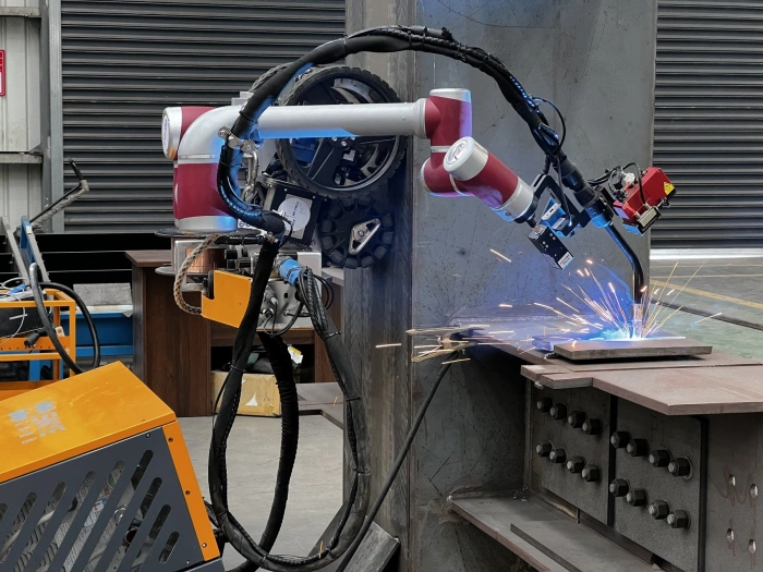
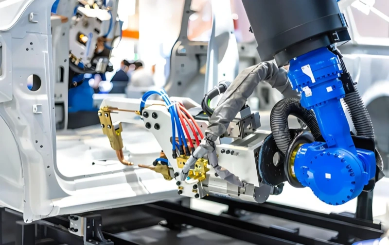
Factory Automation and Robotics
Industrial automation relies on PCBs inside programmable logic controllers, sensor interfaces, and servo drives. These boards process real-time data on factory floors where dust, oil mist, and electrical noise are constant threats. Conformal coating and controlled impedance routing protect signal integrity. A single automation PCB often replaces what used to require an entire cabinet of wired relays, shrinking footprints while boosting throughput.
Medical and Diagnostic Equipment
CT scanners, MRI machines, and patient monitors use high-reliability PCBs that must meet strict IEC 60601 safety standards. These boards often feature HDI technology with microvias to pack dense signal routing into compact enclosures. Failure is not an option when a board powers life-sustaining equipment. Regular cross-section analysis during fabrication verifies plating integrity before these boards ever reach a hospital.
Transportation and Automotive Systems
Rail signaling, electric vehicle charging stations, and avionics all depend on rugged PCBs. These applications subject boards to constant shock, vibration, and wide humidity swings. High-Tg materials like polyimide prevent delamination when soldering temperatures spike during assembly. For more detail on material selection, see our guide on high-temperature PCB materials.
Heavy Equipment and Infrastructure
Mining drills, CNC machines, and grid substation controls use industrial PCBs designed for 15-plus-year service lives. The design process incorporates generous clearances and creepage distances to prevent arcing in dusty or high-altitude installations. You can explore how these designs move from concept to production in our overview of the PCB manufacturing process. For boards requiring extreme durability, heavy copper PCB fabrication provides the current-carrying capacity these systems demand.
How to Choose a Reliable PCB Partner for Industrial Projects
Selecting the right manufacturing partner is as critical as the design itself. These four pillars separate trustworthy industrial PCB suppliers from the rest.
Certifications That Signal Trust
An ISO 9001 certification is the baseline requirement. It proves the manufacturer follows documented quality management processes, not improvised shortcuts. For industrial projects, push further—ask if the facility holds additional certifications like IATF 16949 for automotive-grade traceability or ISO 13485 for medical device compliance. These aren't just wall decorations; they reflect an embedded quality culture that directly impacts your product's field reliability.
Testing Capabilities
Automated optical inspection (AOI) is now standard, but the real differentiator is what happens after surface-level checks. A capable industrial PCB supplier should deploy X-ray inspection to examine hidden solder joints under BGAs and QFNs—defects invisible to optical systems. One factory we audited caught a 2% voiding issue in thermal pads solely through X-ray screening, preventing field failures in a motor controller batch. Ask potential partners for their defect escape rate data and first-pass yield percentages. If they hesitate to share these metrics, treat that as a red flag.
Material Sourcing Transparency
Industrial environments expose boards to thermal cycling, vibration, and chemical contaminants. The laminate choice matters. A reliable PCB manufacturer maintains traceable supply chains for high-Tg FR-4, polyimide, or metal-core substrates, and can provide certificates of conformance for each lot. We've seen projects where substituting a generic equivalent for a specified Rogers material caused impedance shifts that crippled analog performance. Demand visibility into their approved vendor list and incoming inspection protocols.
Production Scalability
A common failure mode is choosing a partner that excels at prototypes but crumbles at volume. Evaluate whether the manufacturer runs dedicated production lines for repeat orders or mixes everything into a shared queue. Consistent output requires calibrated equipment, standardized work instructions, and statistical process control—not tribal knowledge from a single skilled operator. Tour the floor or request a video walkthrough. Look for visual management boards, maintenance logs, and real-time yield dashboards.
Cost Drivers in Industrial PCB Manufacturing
While the base price of a circuit board is driven by its physical dimensions, the final industrial PCB price is a dynamic equation. Three primary variables—material selection, layer count, and testing protocols—can cause the unit cost to swing by over 500%. Understanding these drivers is essential for avoiding over-engineered designs that destroy your budget, or under-specified boards that fail in the field.
100%
-
Material & Substrate
35–45%Laminate, copper foil, prepreg, solder mask, etc.
-
Fabrication & Layer Complexity
20–30%Layer count, lamination, drilling, etching, plating, etc.
-
Testing & Quality Assurance
15–25%AOI, electrical test, X-ray, micro-section, reliability test, etc.
-
Labor & Overhead
10–15%Engineering, setup, handling, facility, utilities, etc.
-
Logistics & Others
5–10%Packaging, shipping, documentation, etc.
| Cost Driver | Impact on Cost | Potential Cost Swing |
|---|---|---|
|
📚
Material Selection
|
High-performance materials (e.g., polyimide, ceramic-filled, high-Tg) can significantly raise raw material cost. | 3x – 5x higher material cost |
|
📐
Layer Count & Complexity
|
More layers mean more lamination cycles, drilling precision, and process steps. | 2x – 3x from 2-layer board to 8-layer board |
|
🛡️
Testing Protocols
|
Advanced testing (100% net test, AOI, X-ray, micro-section, stress screening) adds labor, time, and equipment cost. | 10% – 15% of total board cost |
|
⚙️
Design & DFM Optimization
|
Poor design or ignoring DFM rules can lead to extra layers, special vias, and rework. | 15% – 20% cost increase if not optimized |
| پارامتر | Low-End Consumer PCB | Standard Industrial PCB | High-Reliability Industrial PCB | Mission-Critical PCB |
|---|---|---|---|---|
| Application Example | Simple device (e.g., remote control) | Industrial controller | Medical / Power / Automotive | Aerospace / Defense / Downhole |
| لایهها | 2 Layers | 4 Layers | 8 Layers | 16+ Layers |
| مواد | Standard FR-4 (Tg 130°C) | FR-4 (Tg 150°C) | High-Tg / Low-Loss Material | Polyimide + Ceramic-Filled |
| Testing Level | Basic Flying Probe Test | AOI + ICT Test | AOI + ICT + X-ray | 100% Net Test + Stress Screening + Micro-section |
| Unit Cost Index* | 1.0x (Baseline) | 2.0x – 2.5x | 3.5x – 5.0x | 5.0x – 6.0x+ |
| Cost Difference | — | +100% to +150% | +250% to +400% | +400% to +500% |
Material Selection and Substrate Cost
The single largest cost driver is the laminate. In industrial environments, standard FR-4 is often insufficient. Switching to high-performance materials immediately elevates the PCB cost, but prevents catastrophic failure. For instance, moving from standard FR-4 (Tg 130°C) to a high-Tg polyimide for a downhole drilling tool increases raw material spend by 3x to 5x. However, this is a mandatory investment; a board that de-laminates at 150°C requires costly replacement in an inaccessible location.
Similarly, selecting ceramic-filled hydrocarbon laminates for high-frequency RF and microwave applications minimizes signal loss but significantly impacts cost. The key decision is matching the dielectric constant (Dk) precisely to the application. Over-specifying a low-loss material for a simple motor controller offers zero performance gain while inflating the bill of materials unnecessarily.
Layer Count and Fabrication Complexity
Layer count has a non-linear relationship with cost. A 2-layer board is exponentially cheaper than a 4-layer board, but the jump from 8 to 10 layers is less dramatic proportionally. The primary expense comes from the lamination cycles and the precision required for alignment. A 16-layer backplane for a military radar system involves multiple sequential laminations, where a single misregistration error scraps the entire panel.
This complexity also directly forces you into a heavy copper PCB category if high current is needed on inner layers, which further complicates etching. Rather than routing complex traces across 12 layers, experienced engineers often consolidate signals to reduce the layer stack. A rigorous DFM review at this stage identifies whether blind or buried vias can be eliminated, often cutting costs by 15–20% without sacrificing functionality.
Testing Protocols and Quality Assurance
Testing cost is the final, non-negotiable multiplier. A board destined for a consumer gadget might require only a basic flying probe test for continuity. An industrial PCB for a Class 3 medical ventilator demands far more. The transition from simple Automated Optical Inspection (AOI) to comprehensive electrical testing and micro-sectioning analysis adds significant labor and time.
For critical aerospace or defense orders, customers often mandate 100% net list testing and environmental stress screening. This process detects latent defects like plating voids that would otherwise pass a simple shorts-and-opens test. While these rigorous PCB testing and inspection protocols can represent 10–15% of the total board cost, they are the insurance policy against field failures, where the cost of a recall dwarfs the initial testing investment.
سوالات متداول
Material Selection and Performance
The foundation of any reliable industrial PCB lies in the substrate. Standard FR-4 often falls short in high-temperature or high-frequency environments. For applications demanding superior thermal stability, materials with a high glass transition temperature (Tg > 170°C) are mandatory. In radio-frequency contexts, selecting low-loss materials is critical to maintain signal integrity. A qualified PCB manufacturer will guide you through this selection, but you should verify that the specified laminate meets the thermal and electrical demands of your specific application.
Controlling PCB Fabrication Tolerances
Precision in ساخت برد مدار چاپی directly impacts yield and long-term durability. The complexity of modern designs—featuring fine-pitch components and controlled impedance traces—leaves no room for error. Key tolerances to discuss with your fabricator include minimum trace width and annular ring specifications. Additionally, characteristic impedance control is vital for signal integrity. A rigorous manufacturing partner will provide first-article inspection reports to confirm these parameters before mass production begins.
Breaking Down PCB Assembly Cost
The total PCB assembly cost is driven by three primary levers: component selection, board complexity, and labor. Passives and connectors are straightforward, but specialized ICs and BGAs significantly increase the bill of materials. Furthermore, a design requiring double-sided placement or mixed-technology (through-hole and SMT) adds process steps. To optimize costs without sacrificing quality, engineers should consolidate part numbers and design for automated optical inspection (AOI), reducing manual rework and scrap.
Selecting a Long-Term PCB Manufacturer
Beyond price, the right PCB manufacturer acts as a strategic partner. You need a facility that adheres to IPC-A-600 Class 2 or 3 standards, ensuring visual and structural integrity. Evaluate their quality management system; an ISO 9001 certification is the minimum benchmark, while ISO 13485 or IATF 16949 signals deeper process control. Finally, assess their supply chain transparency. A partner with established laminate and component sourcing strategies protects your production schedule from market volatility and counterfeit risks.
Future Trends Shaping Industrial Electronics
The shift toward smart manufacturing drives a fundamental redesign of industrial electronics. Three interconnected trends are reshaping PCB requirements, demanding a new approach to component selection and board fabrication.
Embedded Components Redefine Density
Miniaturization no longer relies solely on surface-mount advances. Designers now bury passive components—resistors, capacitors, and inductors—directly within the substrate layers. This embedded components strategy frees surface real estate, shortens signal paths, and reduces parasitic inductance. For the procurement specialist, this means evaluating fabricators with laser-drilled cavity expertise and registration tolerances under 25 microns. The result is a cleaner bill of materials and fewer solder joints vulnerable to thermal cycling fatigue.
Industry 4.0 and Intelligent Interconnects
The true backbone of Industry 4.0 is the physical layer connecting distributed sensors, edge gateways, and deterministic actuators. PCBs must now support high-density routing for edge AI processors while maintaining galvanic isolation for 24V field I/O. Real-time Ethernet protocols like EtherCAT and PROFINET demand impedance-controlled differential pairs routed alongside noisy power stages. This convergence forces tighter collaboration between logic and power layout teams, a skill gap many fabricators are still closing. Selecting a partner with mixed-signal design-for-manufacturing (DFM) review capability becomes a non-negotiable supply chain filter.
High-Frequency Demands in Harsh Settings
The push toward millimeter-wave sensing and 5G-connected machinery places high-frequency PCB materials directly on the factory floor. Hydrocarbon-ceramic laminates, once reserved for aerospace, now appear in vibration-prone motor drives and chemical processing nodes. These substrates exhibit a dielectric constant stable within ±0.05 across a -40°C to 125°C range, critical for phased-array predictive maintenance sensors. However, their brittleness introduces drilling and plating challenges absent in standard FR-4. Verifying a fabricator's microvia reliability data for these mixed-material stacks prevents field failures that no conformal coating can remedy.
Ready to Start Your Next Industrial PCB Project?
Every industrial PCB project starts with a clear specification and an experienced manufacturing partner. At PHILIFAST, our engineering team reviews your Gerber files and BOM against our in-house fabrication and turnkey PCB assembly capabilities—catching potential DFM issues early, saving weeks of delay.
⚙ A Single Partner from Prototype to Production
We eliminate variability by keeping your project under one roof—from PCB layout refinement and component sourcing to SMT assembly, conformal coating, and functional testing. One recent motor-drive customer cut their transition from 50-unit prototypes to 5,000-unit production to under four weeks, with zero board respins.
📋 What Your Quote Includes
- Bare PCB fabrication — specified material, surface finish & testing class
- Full turnkey assembly — SMT & through-hole placement
- Component procurement with long-lead-time flagging
- AOI, X-Ray, ICT/FCT per your quality plan
- Final wash, conformal coating & box-build if needed
Comprehensive quotation within 24 hours — backed by a manufacturing review.