

















Large language models are beginning to change PCB design by helping engineers interpret requirements, work with EDA data, and operate design software. They are not yet a substitute for electrical verification, design review, or manufacturing release. The near-term shift is not autonomous PCB production. It is a more capable design assistant – and, in limited cases, an agent – working inside an engineering process that people still govern.
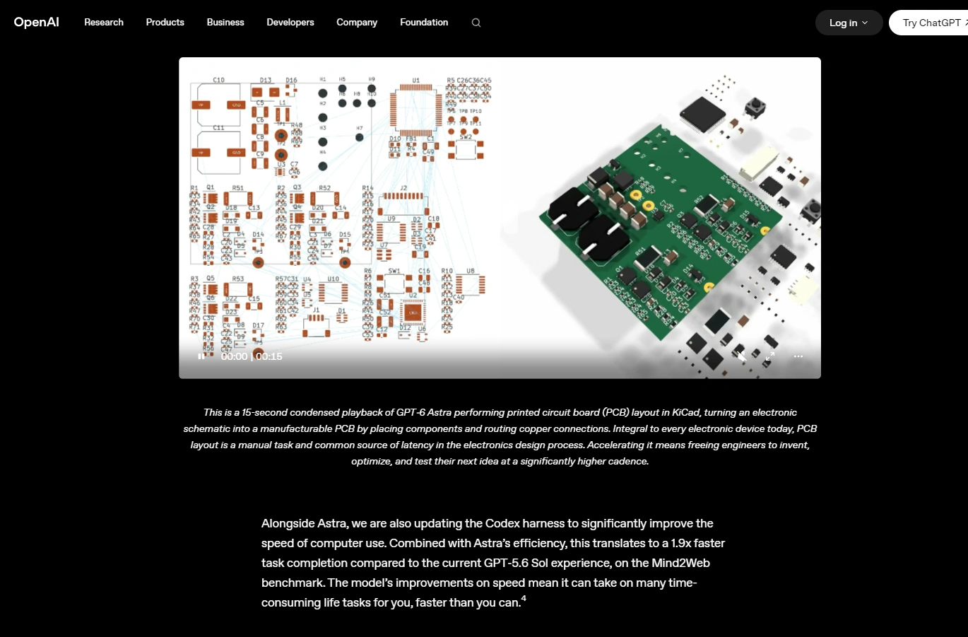
The recent GPT-6 Astra PCB demonstration makes the change tangible. OpenAI shows a condensed playback of Astra using KiCad to turn a schematic into a PCB layout by placing components and routing copper connections. That is meaningful evidence that an agent can operate an EDA environment. It is not evidence that a generated layout has passed simulation, DFM review, assembly validation, or volume-production release.
That distinction is the central issue for AI PCB design: generating a PCB is not the same as validating a PCB.
What changed with modern AI models?
The important change is not that computers can route traces. PCB tools have used rule-driven automation for decades. The change is that foundation models can work across language, documents, code, images, and software interfaces, then follow a multi-step task with tools.
In practical terms, a model can help connect a requirement in plain English to a datasheet, a BOM, a schematic, a footprint library, and an EDA action. A multimodal model can also inspect visual information, such as a schematic page or an EDA screen. A reasoning model can compare options over several steps. An AI agent adds the ability to carry out those steps in software rather than only describe them.
| Approach | Primary strength | Useful PCB-design role | What it does not establish |
|---|---|---|---|
| Traditional CAD automation | Applies explicit, repeatable rules | Interactive routing, constraint checks, library tools, and output generation | Whether the rules capture the full design intent |
| Narrow industrial ML | Recognizes patterns in a defined task | A focused classification or prediction task | Broad engineering understanding or software operation |
| Large model | Connects language, documents, code, and visual context | Requirements analysis, datasheet review, documentation, and design assistance | That every technical inference is correct |
| AI agent | Uses a model to plan and act through tools | Editing EDA data, running checks, and completing bounded workflow steps | That its result is electrically sound or ready to manufacture |
The categories overlap in real products. The useful question is not whether a tool is “AI.” It is what inputs it can read, what actions it can take, how its work is checked, and who approves the result.
What can large models realistically do in PCB design today?
With the right tools and well-controlled design data, large models can already assist with many time-consuming PCB engineering tasks. Their strongest near-term role is to prepare, compare, explain, and iterate – not to make unreviewed release decisions.
Examples include:
- Turning a written requirement into a first-pass checklist of interfaces, rails, constraints, and unanswered questions.
- Reading and comparing datasheets, then identifying differences that an engineer should verify.
- Searching approved component information and drafting BOM notes, alternate-part questions, or lifecycle-risk summaries.
- Generating or modifying structured EDA-related files when the software, file format, and permissions allow it.
- Suggesting placement groupings, routing priorities, or rule candidates from an explicitly supplied constraint set.
- Running software actions, exporting reports, and creating assembly, test, or revision documentation.
- Summarizing DRC, ERC, simulation, or manufacturing-review findings so an engineer can investigate the relevant exceptions.
The PCB layout example in OpenAI’s Astra announcement is one demonstration of software operation. Research is also exploring more specialized workflows. For example, the 2025 ASP-DAC paper PCBAgent describes an experimental high-density placement framework that combines reinforcement learning with an LLM agent. These examples matter because they show a direction of travel, not because they prove a general-purpose production workflow.
Rules and verification tools remain essential. KiCad’s PCB Editor documentation describes DRC as a way to detect defined issues such as missing or incorrect connections, clearance violations, and minimum-width violations. DRC can verify the rules that have been encoded; it cannot determine whether the rule set is complete, whether the circuit architecture is correct, or whether a board will meet every real-world requirement.
Why a generated PCB is not a validated PCB
A layout can be syntactically valid in an EDA tool and still be a poor or unsafe engineering result. Models can miss design intent, rely on incomplete source data, make an unjustified assumption, or produce a plausible explanation for an incorrect decision.
The hard problems are often not visible in a netlist or a screenshot:
- Electrical behavior: power sequencing, stability, protection, timing, analog performance, and fault cases depend on the circuit and operating conditions.
- Signal and power integrity: impedance, return paths, crosstalk, reference-plane transitions, decoupling, and current loops require deliberate constraints and analysis appropriate to the design.
- Thermal and mechanical behavior: component heat, enclosure geometry, airflow, fasteners, connectors, stack-up, and tolerances are not reliably inferred from a short prompt.
- EMC and safety: compliance strategy, grounding, isolation, creepage and clearance, and system-level emissions or immunity need explicit requirements and engineering judgment.
- Supply and library quality: a model may encounter an obsolete part, an unsuitable alternative, an inaccurate symbol, or a footprint that has not been approved.
- Manufacturability: panelization, solder-mask strategy, copper balance, drill choices, assembly clearances, test access, and rework needs depend on the actual fabricator, assembler, design, and production plan.
This is why the release process needs multiple independent checks. The PCB design workflow should connect the schematic, stack-up, constraints, component data, layout, and fabrication outputs before release. Philifast’s complete PCB design workflow guide provides useful context on those design-to-output handoffs.
What a governed AI-assisted release needs
An AI-generated or AI-modified board should be treated as an engineering change. The exact controls vary by product, but a credible release path normally needs the following:
- Defined inputs: a reviewed schematic, approved component data, mechanical envelope, stack-up assumptions, and unambiguous electrical, safety, and manufacturing constraints.
- Tool-based verification: appropriate ERC, DRC, simulation, and specialist analysis for the design’s risks. Passing one check does not replace the others.
- Engineering review: a qualified person reviews architecture, trade-offs, exceptions, and assumptions rather than only accepting an AI summary.
- Manufacturing validation: the fabricator and assembler review producibility, component and process implications, and test or inspection access before a production commitment.
- Traceable approval: the released design, exceptions, revisions, and approval decisions must be identifiable.
について NIST AI Risk Management Framework is not a PCB release standard, but its focus on managing AI-related risk is a useful general reminder: a model’s output needs context, measurement, governance, and documented accountability.
How PCB engineering work may change
AI is more likely to move engineers away from repetitive execution and toward constraint definition, verification, and trade-off decisions than to remove engineers from PCB development. The work does not disappear; the point at which judgment matters moves earlier and becomes more explicit.
Engineer defines requirements and constraints
    -> AI generates or iterates bounded design work
    -> EDA tools and analysis verify defined conditions
    -> Engineer reviews assumptions and exceptions
    -> Fabricator and assembler validate manufacturability
    -> Approved data is released
Routine placement, straightforward routing, documentation, library searching, and first-pass rule checking may become faster. Engineers can spend more time on system architecture, risk, interfaces, physical behavior, verification strategy, and the constraints that determine whether an automated result is acceptable.
This makes design intent more valuable, not less. A well-phrased prompt is useful, but it is not a complete specification. An agent needs machine-readable constraints, approved libraries, tool access, and clear stop conditions. The better those inputs are, the more safely the agent can help.
For teams designing for testing, assembly, and service from the beginning, DFM, DFA, and DFT considerations should become part of that constraint package rather than a late-stage review.
Why PCBA manufacturing becomes more important, not less
As design generation becomes easier, the value of reliable manufacturing feedback rises. A layout can be optimized only against information the system has: actual component availability, fabricator rules, assembly process limits, inspection results, test failures, and controlled revision history.
The promising future direction is a feedback loop, not a one-way handoff:
Design -> DFM -> Fabrication -> SMT assembly -> Inspection -> Testing
    -> Production data -> AI-assisted analysis -> Design improvement
In a mature version of this loop, a future design agent might learn from approved, traceable data about recurring assembly constraints, component substitutions, test escapes, rework patterns, or thermal findings. It could propose a better placement, a more testable layout, or a manufacturing question for the next revision.
That is an emerging direction, not a standard PCBA workflow today. It only becomes useful when the data is tied to the right board revision, component revision, process conditions, inspection method, and test definition. Raw yield data without that context can teach an AI system the wrong lesson.
Manufacturing expertise remains necessary wherever a board must be fabricated and assembled under a defined process. That process knowledge helps translate a design into buildable product. A prototype-to-production PCB assembly plan and a defined PCBA testing approach are examples of information that must stay connected to the board, even when AI assists the design work.
Philifast — PCB Design to Manufacturing Support
We help translate AI-assisted designs into validated, manufacturable PCBAs with reliable feedback.
What PCB and PCBA manufacturers may need to provide
In an AI-assisted design ecosystem, the strongest manufacturing input is structured, usable engineering knowledge – not a vague statement that a board is manufacturable. Manufacturers may increasingly be asked to expose constraints and feedback in forms that people and software can both use.
Useful inputs could include:
- machine-readable DFM rules tied to a stated process capability;
- approved stack-up and material options for the actual board requirement;
- clear assembly keep-outs, panel, fiducial, stencil, and test-access constraints;
- component, finish, and process assumptions attached to the revision being reviewed;
- traceable records of review findings, approved exceptions, inspection, and test results;
- structured feedback that distinguishes a design issue from a component, process, or test issue.
Not every manufacturer will expose all of this data, and not every project needs it. The point is architectural: an agent cannot reliably optimize against manufacturing knowledge that exists only in scattered emails, tribal knowledge, or an ambiguous quote note.
From AI assistant to engineering agent: a realistic progression
The path to closed-loop electronics engineering has several stages. Treating them as one thing leads to exaggerated claims.
| Stage | What AI can do | Main limitation | What must improve next |
|---|---|---|---|
| AI assistant | Explain concepts, search documents, draft checklists, and summarize reports | It may be inaccurate and cannot reliably act in the design environment | Grounding in approved project data and reviewable citations |
| AI copilot | Help edit files, compare components, propose constraints, and perform bounded EDA tasks | Its actions still need frequent engineering review | Reliable tool integration, permissions, and repeatable evaluations |
| AI agent | Execute multi-step tasks in EDA and engineering tools under defined limits | It can follow flawed or incomplete intent and may not detect physical risk | Better verification, constraint models, and safe handoffs |
| Closed-loop engineering | Connect design, DFM, production, inspection, test, and revision feedback | This is not a mature general-purpose workflow | Structured data, traceability, validated feedback, governance, and accountability |
The organizational barrier is as significant as the technical one. Engineering teams need to decide which actions an agent may take, which it may propose only, what evidence is required for approval, and how an exception is recorded. These are product-development governance questions, not merely software configuration.
Could AI eventually design a PCB and send it directly to manufacturing?
AI could eventually prepare a highly complete manufacturing package for bounded designs, but direct autonomous release to manufacturing is not yet a reliable general practice. Sending files is easy. Establishing that the files embody the right design intent, meet the relevant constraints, and are approved for the intended build is the difficult part.
Before such a workflow can be trusted, it needs at least:
- machine-readable specifications and acceptance criteria;
- validated symbols, footprints, and component models;
- approved component and lifecycle data;
- electrical, mechanical, thermal, EMC, and safety constraints appropriate to the product;
- EDA checks and analysis selected for the design risk;
- fabricator and assembler rules for the chosen process;
- human approval for consequential release decisions; and
- revision-linked manufacturing, inspection, and test feedback.
The likely bottleneck is therefore moving from drawing a PCB to defining, validating, and governing the constraints under which an AI system works. When those constraints are weak, automation can make a bad decision faster. When they are strong, it can reduce repetitive work and surface better questions earlier.
よくあるご質問
Can large language models design PCBs today?
They can assist with PCB design and, when connected to suitable tools, can perform bounded actions such as editing design data, placing components, routing connections, or running checks. A generated design still needs engineering verification and manufacturing review before release.
How is AI PCB design different from traditional PCB automation?
Traditional automation follows explicit rules in the EDA tool. AI PCB design can interpret text, documents, visual information, and tool results across a workflow. That broader context is useful, but it also introduces the risk of incorrect assumptions, so verification remains necessary.
Can AI replace PCB engineers?
Not in the foreseeable workflow described here. AI can reduce routine work, but engineers remain responsible for architecture, constraints, safety, physical behavior, trade-offs, verification, and release decisions.
Can an AI agent send a PCB directly to a manufacturer?
An agent can transmit files if it has the necessary integration and permission. That does not make the package suitable for manufacturing. A controlled release still needs validated data, agreed manufacturing requirements, and accountable approval.
How could PCBA data improve future PCB designs?
When inspection, test, sourcing, and production records are accurately linked to the correct revision and process context, they can reveal recurring issues for engineers to investigate. AI may help analyze that information and propose changes, but it should not infer causation or approve a revision without review.
The practical takeaway
Large models can make PCB engineering more conversational, more automated, and more iterative. Their real value will come from working with engineering tools and trustworthy manufacturing inputs – not from bypassing verification.
For PCB and PCBA teams, the immediate opportunity is to improve the quality of requirements, libraries, constraints, review records, and production feedback. That work makes current engineering stronger and creates the conditions for AI assistance to become genuinely useful.
Philifast — AI-Ready PCB Manufacturing
Partner with us to build reliable, manufacturable boards while you adopt AI-assisted design workflows.