


배경
레진 충전 비아 공정은 PCB 제작에 점점 더 많이 사용되고 있습니다. 레이어가 많은 보드와 고정밀 PCB에서 흔히 사용됩니다. 레진 충진은 솔더 마스크 플러깅이나 라미네이션 필러 레진이 해결할 수 없는 많은 문제를 해결할 수 있습니다. 동시에 이 공정에 사용되는 레진은 특별한 특성을 가지고 있습니다. 이러한 특성으로 인해 보드 제작 단계에서 많은 어려움이 있습니다.
정의
레진 플러깅은 레진을 사용하여 내부 레이어에 매립된 비아를 채운 다음 라미네이션을 수행하는 것을 의미합니다. 이 방법은 고주파 보드와 HDI 보드에 널리 사용됩니다. 전통적인 스크린 인쇄 레진 플러깅과 진공 레진 플러깅의 두 가지 주요 유형이 있습니다. 대부분의 제품은 전통적인 스크린 인쇄 수지 방식을 사용합니다. 이는 업계에서 가장 일반적인 방법이기도 합니다.
PCB에서 “플러그드 비아”란 무엇인가요?
기능 및 업계 요구 사항을 통해
비아(도금 스루홀, PTH)는 보드의 여러 레이어를 연결합니다. 전자 산업의 성장은 PCB 기술을 발전시키고 있습니다. 또한 더 나은 보드 제작 및 표면 실장 작업에 대한 필요성도 높아졌습니다. 플러그 비아 공정은 이러한 요구를 충족하는 것으로 보입니다. 플러깅은 이러한 규칙을 충족해야 합니다:
비아 내부에 구리가 있어야 합니다. 비아는 솔더 마스크 아래에 채워지거나 채워지지 않을 수 있습니다.
비아 내부에는 일정한 두께(예: 4μm)의 땜납(주석-납)이 있어야 합니다. 솔더 마스크 잉크가 구멍에 들어가서 솔더 비드가 갇히지 않아야 합니다.
비아는 빛이 통과하지 못하도록 솔더 마스크로 덮어야 합니다. 구멍에 납땜 링이나 납땜 비드가 없어야 합니다. 채워진 구멍은 평평해야 합니다.
전자 제품이 더 가볍고, 더 얇고, 더 짧고, 더 작아짐에 따라 PCB도 고밀도, 고난이도로 이동하고 있습니다. 이로 인해 많은 SMT 그리고 BGA 보드. 고객이 부품을 조립할 때 종종 플러그형 비아를 요청합니다. 플러그는 크게 다섯 가지 용도로 사용됩니다:
웨이브 솔더링 중에 솔더가 비아를 통과하여 부품 측이 단락되는 것을 방지합니다. 이는 비아를 BGA 패드에 배치할 때 중요합니다. 그런 다음 먼저 플러그를 꽂은 다음 금도금을 하면 BGA 납땜이 더 쉬워집니다.
비아 내부에 플럭스 잔여물이 남지 않도록 합니다.
표면 실장 및 조립 후 진공 픽 앤 플레이스 또는 진공 테스트 단계를 수행할 수 있습니다. 진공이 작동하려면 밀폐된 상단이 필요합니다.
페이스트가 비아로 흘러들어가 납땜 조인트가 약해지거나 배치가 불량해지는 것을 방지합니다.
웨이브 솔더링 중에 솔더 볼이 튀어나와 단락을 일으키는 것을 방지합니다.
레진 충진 비아의 장점
BGA가 있는 다층 기판에서 레진 플러깅은 비아 사이의 간격을 줄일 수 있습니다. 이는 라우팅 및 트레이스 레이아웃에 도움이 됩니다.
내부 HDI 레이어에 매립된 비아의 경우 레진 필은 라미네이션 중 프리프레그의 두께 제어와 매립 비아의 레진 필 설계의 균형을 맞추는 데 도움이 됩니다.
관통 구멍이 큰 두꺼운 보드의 경우 레진 충진으로 제품 안정성이 향상됩니다.
레진으로 채워진 비아는 BGA 부품 때문에 자주 사용됩니다. 기존 BGA에서는 비아가 패드에서 뒷면으로 라우팅될 수 있습니다. BGA가 조밀하여 비아가 라우팅되지 않는 경우 패드에 비아를 뚫고 다른 레이어로 라우팅할 수 있습니다. 그런 다음 구멍을 레진으로 채우고 구리를 도금하여 패드로 만듭니다. 이를 VIP 프로세스(비아 인 패드)라고 합니다. 패드에 비아를 뚫고 레진 필을 사용하지 않으면 땜납이 누출되어 패드에 뒷면 단락 또는 조인트 불량 문제가 발생할 수 있습니다.
레진 충진 비아의 공정 흐름
일반 레진 충진 공정:
구멍을 뚫습니다.
구리로 구멍을 뚫어 플레이팅합니다.
레진으로 구멍을 채우고 굽습니다.
평평하게 갈거나 밀링(평면화)합니다.
연마 후 수지 부분에는 구리가 없습니다. 그런 다음 채워진 부분을 패드로 바꾸려면 새로운 구리 도금 단계가 필요합니다. 이 도금 단계는 다른 구멍에 대한 일반 드릴링 전에 수행됩니다. 요컨대, 먼저 채워질 비아를 처리한 다음 다른 구멍을 뚫고 정상적인 흐름을 따르십시오.
다음은 공장에서 볼 수 있는 몇 가지 주요 단계와 스테이션입니다:
VIP 도금 및 패널 연마
알루미늄 시트 스크린/패드
보드 제작용 알루미늄 시트 및 패드 보드 장착
인쇄 필름 정렬 테스트 및 잉크 혼합
평가판 인쇄
NG 라인 자체 점검, 배치 생산, 섹션 경화 가능
IPQC 샘플링
세라믹 패널 연삭
외부 레이어 및 포토 필름 조건
외부 레이어 작업이 네거티브 필름 제한을 충족하고 PTH 종횡비가 6:1 이하인 경우:
충족 조건: 선폭과 간격이 충분히 크고, 최대 PTH 홀이 드라이 필름 밀봉 한계보다 작고, 기판 두께가 드라이 필름 최대 두께보다 작으며, 국부 무전해 금, 니켈-금 기판, 하프홀 기판, 플러그인 기판, 환형 PTH 또는 PTH 슬롯 홀이 없는 등의 특별한 요구 사항이 없는 경우입니다.
표준 내부 레이어 제작 → 라미네이션 → 브라운 산화물 → 레이저 드릴링 → 디브라운 → 외부 드릴링 → 침지 구리 → 패널 충전 전기 도금 → 단면 분석 → 외부 패턴 → 외부 산성 에칭 → 외부 AOI → 일반 흐름을 따릅니다.
외부 레이어가 네거티브 필름과 만나지만 PTH 종횡비가 6:1을 초과하는 경우:
화면비가 6:1을 초과하는 경우, 전체 패널 비아 필 도금으로는 비아에 필요한 구리 두께에 도달할 수 없습니다. 패널 필 도금 후 비아 구리 두께를 늘리려면 두 번째 전체 기판 전기 도금이 필요합니다. 흐름:
내부 레이어 제작 → 라미네이션 → 브라운 산화물 → 레이저 드릴링 → 탈브라운 → 외부 드릴링 → 침지 구리 → 패널 충전 전기 도금 → 전체 패널 전기 도금 → 단면 분석 → 외부 패턴 → 외부 산성 에칭 → 일반 흐름을 따릅니다.
외부 레이어가 네거티브 필름을 충족하지 않지만 선 너비/갭이 a 이상이고 외부 PTH 종횡비가 6:1 이하인 경우:
내부 레이어 제작 → 라미네이션 → 브라운 산화물 → 레이저 드릴링 → 디브라운 → 외부 드릴링 → 침지 구리 → 패널 충전 전기 도금 → 단면 분석 → 외부 패턴 → 외부 전극 → 외부 알칼리 에칭 → 외부 AOI → 일반 흐름 따르기.
외부 레이어가 네거티브 필름을 충족하지 않거나 선 너비/갭 < a 또는 선 너비/갭 ≥ a이지만 PTH 종횡비가 6:1을 초과하는 경우:
내부 레이어 제작 → 라미네이션 → 브라운 산화물 → 레이저 드릴링 → 탈브라운 → 침지 구리 → 패널 충전 전기도금 → 단면 분석 → 구리 환원 → 외부 드릴링 → 침지 구리 → 풀 패널 전기도금 → 외부 패턴 → 패턴 전기도금 → 외부 알칼리 에칭 → 외부 AOI → 정상 흐름 따르기.
단면 및 품질 참고 사항
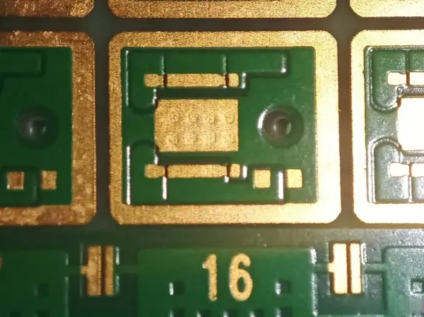
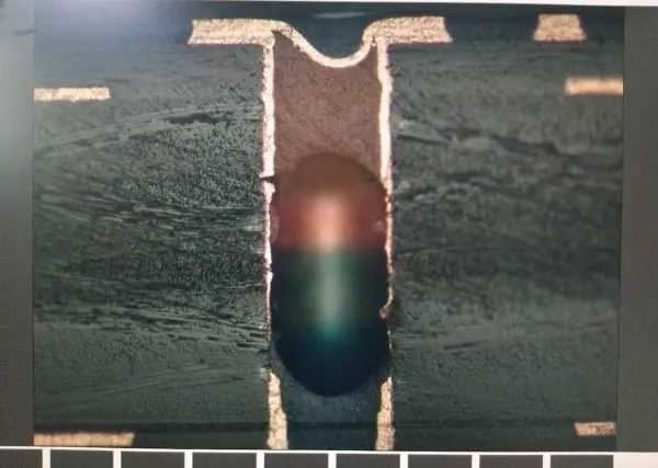
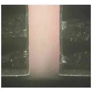
수지 플러그 단면
단면 분석 결과, 레진 잉크가 잘 꽂힌 비아는 레진이 완전히 채워진 것을 보여줍니다. 레진이 구멍을 100%까지 채웁니다. 상단과 하단의 레진 표면은 균일하게 약간 볼록합니다. 그 후 세라믹 패널 연삭을 통해 표면을 평평하게 만듭니다.
충전 품질 및 점검
레진 충전물은 빈 공간 없이 꽉 채워야 합니다.
연마 후 플러그 표면은 평평해야 합니다.
비아 구리는 최종 전기 도금 후 두께 규칙을 충족해야 합니다.
납땜 볼이나 납땜 링이 갇혀 있는지 확인합니다. 이런 것들이 있으면 안 됩니다.
마스크나 커버를 덮은 후 플러그가 빛을 투과하지 않는지 확인하세요.
실용적인 참고 사항 및 모범 사례
VIP(비아 인 패드) 작업의 경우, 일반 드릴링 및 기타 단계 전에 비아 충진 작업을 수행하고 해당 지점에 패드를 만듭니다. 이렇게 하면 잘못된 공정을 방지하고 최종 도금 품질을 높일 수 있습니다.
보드에 매립형 또는 블라인드 비아가 많은 경우, 라미네이션 두께를 안정적으로 유지하기 위해 패드와 채우기 단계를 계획합니다.
적절한 레진 유형과 경화 프로파일을 사용합니다. 레진 선택은 흐름, 경화 및 연삭 동작에 영향을 미칩니다.
패널 충전 단계 후 IPQC 샘플링 및 단면 검사를 사용하여 비아 내부의 구리 및 레진 충전 품질을 확인합니다.
AOI 및 기타 최종 테스트를 통해 솔더 마스크 또는 페이스트 문제가 남아 있지 않은지 확인합니다.
요약
레진 충전 비아는 최신 HDI 및 BGA 보드의 핵심 공정입니다. 라우팅을 돕고, 신뢰성을 개선하며, 납땜 결함을 방지합니다. 드릴링, 도금, 레진 충진, 베이킹 및 연삭을 신중하게 제어해야 합니다. 레진 플러깅을 잘 계획하면 VIP 디자인을 사용하고 타이트한 BGA 패드 요구 사항을 충족할 수 있습니다.