
PCB fabrication · Filled & capped vias
Resin-Filled Via
PCB Manufacturing
A plated connection inside. A supported soldering surface above.
FLJ manufactures PCBs with resin-filled and copper-capped vias for via-in-pad assembly. From prototype boards to production, filling, curing, planarization and copper capping turn a plated hole into part of the component land.
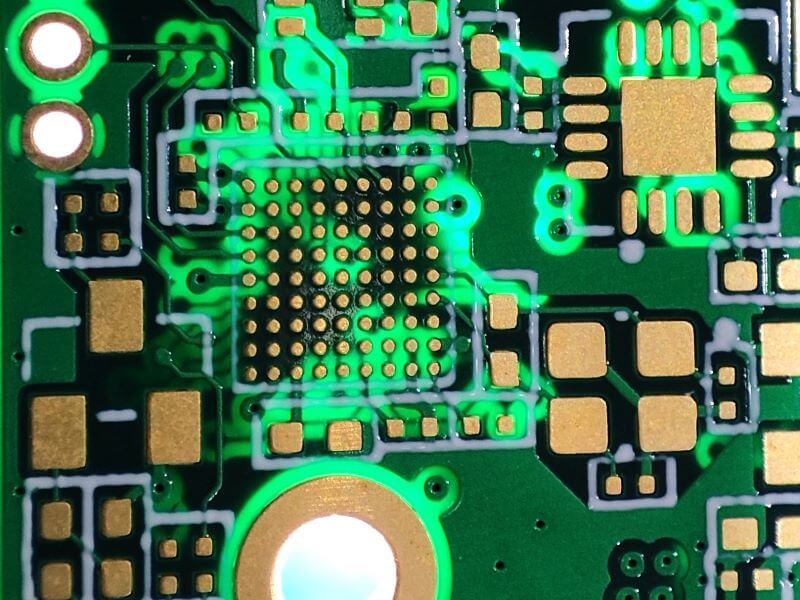
The finished land
Resin-Filled Vias for Via-in-Pad Assembly
An open via in a soldering land gives molten solder a path into the board. Resin filling and copper capping close that path while retaining the plated connection between layers.
Copper Barrel, Resin Fill and Copper Cap
The copper barrel connects the selected copper layers. Non-conductive resin occupies the remaining bore and provides support for the metal deposited across the opening. The copper cap then creates the surface on which the component can be soldered.
These parts work together: filling the bore does not remove the electrical connection, and filling alone does not create a solderable metal pad. Via-in-pad plated over, or VIPPO, combines the in-pad position with a filled hole and plated-over surface.
Component Lands and Routing Space
Placing a via within a BGA land frees space that an external fan-out connection would otherwise occupy. It is particularly useful where the pad arrangement leaves little room for a separate via and connecting trace. The filled and capped surface also prevents the hole opening from draining solder from the joint.
Filled-and-capped thermal vias within an exposed component pad can also close the solder-drain path. Here, the resin supports the soldering surface while the plated copper provides a heat-conduction path. The number and arrangement of vias, copper thickness and connection to the rest of the thermal structure determine how that path contributes to cooling. FLJ supplies fabrication and BGA assembly so the finished lands and soldering process can be considered together.
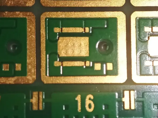
From plated bore to finished pad
Resin Filling and Copper Capping: The Manufacturing Process
Each operation prepares the next: plating establishes the connection, cured resin supports the opening, and planarization prepares a surface for copper capping.
Form and Plate the Hole
Drilling establishes the hole geometry. Hole-wall preparation removes drilling residues before metallization and copper plating form the conductive barrel. Where the hole intersects an intended inner-layer land, that copper connection must remain continuous.
The drilled diameter is not the empty bore available for resin after plating. Copper deposited on the wall reduces that opening. Hole depth, remaining bore and copper thickness therefore influence the filling process together.
Drill diameter describes the hole before wall plating. The remaining bore is smaller once copper has been deposited.
Illustrative plan views; not to scale.
Fill the Bore and Cure the Resin
The filling operation places resin through the plated bore while controlling trapped air and incomplete penetration. Resin flow, hole geometry and the filling method determine how effectively the material reaches the full hole depth.
Thermal curing hardens the resin before the filled surface is machined and capped. An under-cured fill can change during later heating, while an air pocket leaves part of the cap without solid support beneath it. The cure schedule follows the selected resin and board construction.
Plating a metal cover over the opening does not correct incomplete filling below it. Filling and curing therefore establish the internal support before the process turns to surface level and copper coverage.
Planarize the Filled Surface
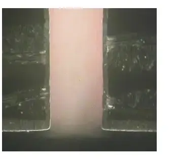
Excess cured resin is removed from the board surface. Planarization brings the fill into line with the surrounding copper while preserving the copper needed for the final land. This controls both raised fill and depressions over the opening.
A filled hole can still present an unsuitable mounting surface if it protrudes or sits below the surrounding copper. The surface must be prepared before a continuous copper cap is formed.
Excess resin remains above the opening.
Excess is removed to prepare a level surface.
Copper joins the land across the supported opening.
Add the Copper Cap and Final Finish
The prepared filled surface is metallized and copper plated to bridge the opening and join the surrounding land. The cap provides a continuous metal surface over the resin. Subsequent circuit processing defines the required land, and the selected surface finish protects the exposed soldering surface.
A gold-colored final finish is not itself the copper cap. The cap is part of the copper construction beneath that finish. Its continuity and the finished surface level both matter to the component joint.
Inside the hole · Across the land
Inspection of the Fill, Copper and Pad Surface
A satisfactory surface appearance does not establish that the fill is sound throughout the hole. Inspection addresses the internal structure and the mounting surface separately.
Internal Fill and Copper Integrity
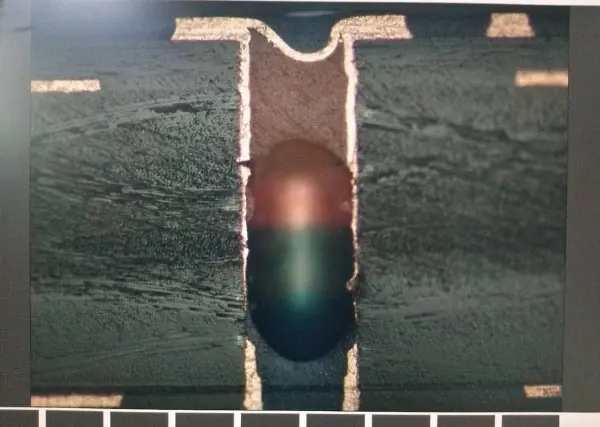
A representative coupon or selected board area is mounted, ground and polished to expose a section through the hole. The section makes fill penetration, voids, separation at the resin-to-copper interface, barrel copper and cap continuity visible in that plane.
A void beneath the cap and a break in the copper barrel are different findings: one affects support, while the other can interrupt the electrical path. Sectioning is destructive and examines the prepared plane, so its result describes that sampled location.
Bare-board electrical testing checks opens and shorts in the conductive network. It complements the construction checks; it does not establish the condition of non-conductive resin inside a passing connection.
Surface Level and Cap Continuity
Surface inspection checks for exposed resin, discontinuous copper, protrusion and depression relative to the surrounding land. Height measurement evaluates the surface geometry rather than relying on color or reflected light alone. The finished pad must present a usable soldering surface for the intended component.
Quoting the actual construction
Cost Factors for Resin-Filled and Capped Vias
The added work is more than the resin itself. Filling, curing, planarization, surface preparation and copper capping all contribute to the fabrication route.
Request a filled-via PCB quoteFill Material, Selected Holes and Process Work
The selected compound and the depth and diameter of the plated bore influence how the holes are filled. A long, narrow bore presents a different filling task from a shorter, wider opening. Hole count matters, but it does not describe that geometry or the surface work by itself.
Filling selected buried vias before the remaining layers are laminated places the filling operation inside the build-up sequence. Filling and capping an outer assembly land adds the work needed to finish a usable metal surface. The drawing should distinguish those jobs rather than marking every hole with one undifferentiated fill note.
Surface and Verification Needs
Copper-capped assembly lands require the additional surface operations associated with VIPPO. Surface geometry, construction inspection and any specified reliability work also affect the manufacturing effort. There is no single price multiplier that describes every filled-via board.
Send the Gerber or ODB++ data, drill file, stackup, quantity and filling notes. Identify the vias to fill and whether copper capping is required. FLJ can quote the board with the relevant fill and surface construction.