


In PCB design, routing can be seen in three broad levels. The first level is basic connectivity. This is the most basic demand in PCB design. If the nets do not connect, the board has no fundamental function. Then the board is a scrap. Do not talk about other things.
The second level is performance. This is the measure of how good a printed circuit board is. After routing, we must think about how to reach the best performance. We must avoid different kinds of interference. We must also keep signals stable and clean.
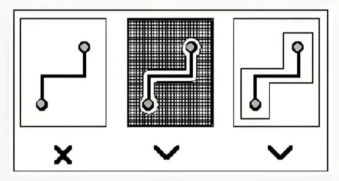
The third level is appearance. The traces may connect and the board may show good electrical performance, but the layout can still look messy. In that case, we should make the routing look neat. Neat routing helps later testing and repair. Neat routing also shows the skills of a senior engineer.
How to route well
Routing methods can vary a lot. To avoid problems such as reflected signals when input and output traces run close and parallel, and to avoid parasitic coupling when traces on two adjacent layers run parallel, we must think about many factors. If interference is strong enough, the board may not work at all. Below are some recommended rules for PCB routing.The “five-five” rule (layer choice rule)
This rule helps choose the number of PCB layers. When the clock frequency reaches 5 MHz or the pulse rise time is less than 5 ns, the PCB should be a multilayer board. This is a common rule.
Sometimes people still choose a two-layer board due to cost. If you use two layers, try to use one full side as a solid ground plane. That helps performance.
Mixed digital and analog ground rules
Now many PCBs have both digital and analog circuits. When routing, think about interference between them, especially noise on the ground. Digital circuits work at high frequency. Analog circuits are often sensitive.
For signals, keep high-frequency traces far from sensitive analog parts. For ground, the whole PCB has one node to the outside world. So you must treat digital and analog grounding inside the board carefully.
Inside the board, digital ground and analog ground are often separate and not connected to each other. They only join at the point where the PCB connects to the outside world, such as a connector. Make sure digital ground and analog ground have a short link at a single point. Some systems may choose not to share ground on the board. Follow the system design decision.
Handling component leads in large copper areas
Large copper ground or power areas often meet many component leads. For handling part leads we must balance electric performance and assembly.
From an electrical view, a pad should be fully connected to copper for best performance. But full copper pads create problems in soldering. Problems include:
Soldering needs a lot of heat from the soldering iron.
It is easier to get cold or weak solder joints.
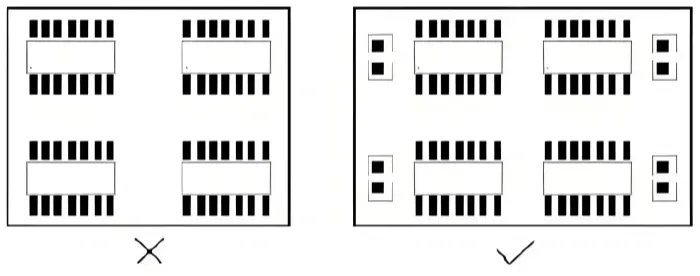
To balance electrical needs and manufacturing, make thermal relief pads. A common form is a cross-shaped pad. This is called thermal relief or thermal pad. It helps soldering by isolating the pad thermally from large copper planes. Thermal pads reduce the chance of cold solder joints. Treat vias connecting to power and ground layers the same way in a multilayer board.
Grid system rules
A grid ground system or mesh ground helps reduce trace inductance and gives a good return path for RF currents. But be careful with grid density.
If the grid is too dense, there will be many small mesh steps. That generates a lot of layout data. This needs more storage and slows CAD tools. Also some grid paths are useless because they are taken by component pads or mounting holes. If the grid is too sparse, routing becomes hard and routing success falls.
So choose a reasonable grid density. Standard component lead spacing is 0.1 inch (2.54 mm). So a base grid of 0.1 inch or a neat submultiple is common. Examples: 0.05 inch, 0.025 inch, 0.02 inch, and so on.
How to check after routing
After finishing PCB routing, check whether the design follows the rules and whether it meets manufacturing limits. The checks below are common.
Areas to check include: general PCB design drawing items, PCB electrical checks, PCB physical checks, mechanical design factors, PCB mounting requirements, board breakout needs, mechanical considerations, electrical concerns, routing paths and placement, trace widths and thickness, trace spacing, trace shape checks, and a list of design items.
Practical checklist
Check if the distance between vias is reasonable.
Check if power and ground trace widths suit current needs.
Check whether key signal traces use the best measures (short path, controlled impedance, shielding).
Check whether analog and digital parts have separate grounds if needed.
Check whether added copper patterns on the board could short signals.
Check whether the board has required fabrication lines or markings for the factory.
Check whether the power and ground plane edges in a multilayer board have the required inset.
Routing case study and key rules
Routing is a major part of PCB design. Routing often takes the most time. Engineers should follow basic rules when routing, such as chamfer rules and the 3W rule.
Ground loop rule
The smallest loop rule means the area enclosed by a signal and its return path should be as small as possible. The smaller the loop area, the less the board will radiate and the less it will receive external noise.
When splitting ground planes, think about how the plane shape and important signal paths align. Prevent problems from ground plane slots that increase loop area.
On two-layer designs, keep enough area for power. Fill other space with reference ground copper. Add necessary ground vias to connect the two sides of the board. For key signals, use ground isolation. For high-frequency designs, use multilayer boards.

Shielding and protection rule
Shielding is another way to reduce loop area and lower radiation. Use shielding for important signals such as clock and sync signals.
For very critical or very high-frequency signals, you can use a copper shield or coax-like design. Surround the routed trace on all sides with ground. Also plan how the shield ground connects to the main ground plane.
Crosstalk control rule
Crosstalk means interference between different nets on the PCB. It comes from long parallel routing. The cause is distributed capacitance and inductance between parallel traces.
Main ways to fight crosstalk:• Increase spacing between parallel traces. Follow the 3W rule.• Insert grounded guard traces between critical parallel traces.• Reduce the distance between the routing layer and the ground plane.
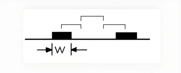
3W rule reminder
To cut crosstalk, keep trace spacing large. If the center distance is three times the trace width, about 70% of the field is isolated. For 98% isolation, use 10W.
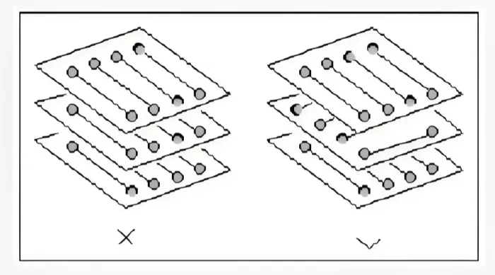
Direction control of traces
Keep the direction of adjacent layers orthogonal. Avoid running traces in the same direction on adjacent layers. This reduces layer-to-layer coupling. If board structure forces parallel runs, especially in high-speed designs, use ground planes between routing layers to isolate them. Also use grounded guard traces between signal traces.
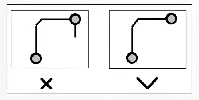
Dangling trace check rule
Do not leave any net end floating without connection. Floating traces can act as antennas. They cause extra radiation and they can pick up noise. Avoid this.
Closed loop check rule
Prevent a signal from forming a loop across different layers. In multilayer boards, loops cause radiation. Watch for this and adjust routing.
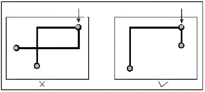
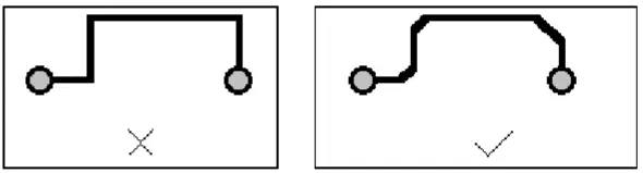
Chamfer rule
Avoid acute or sharp angles in trace corners. Sharp corners can cause unwanted radiation. They can also be poor for manufacturing. Use gentle turns or 45-degree angles.
Decoupling components rule
Add decoupling capacitors as needed. Decoupling filters noise on the power lines. Place the decoupling capacitor close to the device power pin after the power filter.
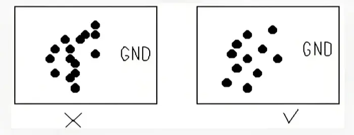
Integrity of power and ground planes
In areas with many vias, do not let vias cut the plane so that the plane separates into smaller parts. Plane splits raise loop area and cause signal return path problems. When you fanout, keep via spacing so that you can still route at least one trace between vias.
Power plane overlap rule
Avoid overlap of different power planes in space. This reduces interference between supplies, especially when different supplies have large voltage differences. If overlap is unavoidable, consider adding a ground layer between them.

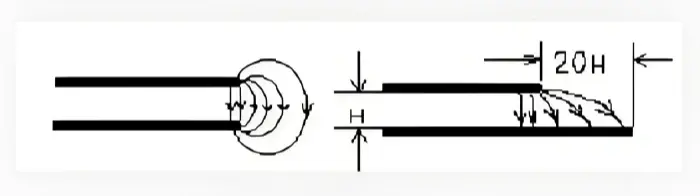
20H rule repeated
Remember the edge effect. Power to ground plane spacing affects edge radiation. Inset the power plane to keep the field inside the ground plane. An inset of 20H limits about 70% of the field. An inset of 100H limits about 98% of the field.
More detailed routing rules and checks
Return path control
Always plan the signal return path. A signal must have a low-impedance return beneath it. Keep ground return paths short.
Fanout and via planning
For dense BGA or fine pitch parts, plan fanout early. Keep via spacing that leaves room to route signals. For fanout, use microvias or blind vias if needed in advanced designs.
Impedance control
For high-speed single-ended traces or differential pairs, control the trace width and spacing to match the target impedance. Use the PCB stack-up and dielectric to calculate trace geometry.
Differential pair routing
Route differential pairs with equal length. Keep the spacing stable. Avoid stubs. Keep bends smooth.
Length matching and delay
For buses and interfaces needing matched timing, match the routing length. Use serpentine traces for length tuning. Keep serpentine patterns smooth and short in height.
Thermal relief and thermal pads
When attaching pads to large copper, use thermal relief. Make the pad connect to the plane with spokes. This helps soldering.
Solder mask and paste mask
Check solder mask openings. Align paste mask for SMD parts. Make sure small pads have correct paste area.
Design for test and assembly
Leave test points and assembly markers. Keep space for probes. Make placement allow soldering and inspection.
Final routing checklist (short list)
• Check all nets are connected.• Run DRC and ERC checks.• Check trace width and current.• Check spacing for crosstalk and voltage.• Check decoupling and bulk capacitors.• Check plane splits and return paths.• Check thermal reliefs and pad shapes.• Check assembly and test access.
Common errors to avoid
• Leaving ground plane slots under critical signals.• Running high-speed traces next to noisy power traces.• Using many 90-degree corners.• Not adding decoupling near IC pins.• Letting vias split planes badly.• Not planning fanout for dense chips.
Closing notes
Routing is a key part of PCB design. A good routing job gives correct connections, good performance, and good appearance. Follow simple rules. Keep loops small. Control crosstalk and return paths. Use plane insets for edge control. Use decoupling for power noise. Use thermal reliefs for soldering. Use a reasonable grid for routing. Check the board carefully after routing.
If you follow these basic rules, you will reduce EMI, improve signal quality, and make the board easier to build and maintain. Routing needs care. Spend time at planning and layout. Good layout pays off in time saved in test and repair, and in the final product quality.

