


Aluminum PCB Design Guide: Optimizing Heat Dissipation for Power Electronics.
Power electronics generate significant heat—and when that heat isn’t properly managed, performance degrades, components fail prematurely, and entire systems can shut down. مركبات ثنائي الفينيل متعدد الكلور الألومنيوم solve this challenge by integrating a metal core directly into the circuit board structure, creating a thermal highway that moves heat away from sensitive components far more efficiently than traditional FR-4 boards.
Unlike conventional PCBs that rely on fiberglass substrates with poor thermal conductivity (around 0.3 W/mK), aluminum PCBs feature a metal base that conducts heat 5-10 times more effectively. This fundamental difference transforms how designers approach thermal management in LED lighting, motor controllers, power converters, and automotive electronics—applications where heat dissipation directly impacts reliability and lifespan.
The thermal advantage extends beyond just the substrate material. Design elements like trace width, copper thickness, and dielectric layer selection all work together with the aluminum base to optimize heat flow. Research shows that proper thermal design can reduce operating temperatures by 30-50°C compared to standard boards—a difference that dramatically extends component life in high-power applications. Understanding how aluminum PCBs manage thermal stress sets the foundation for effective design decisions that balance performance, cost, and manufacturability.
Components of Aluminum PCBs: Structure and Material Benefits
Understanding the layered architecture of aluminum PCBs reveals why they excel at thermal management. Unlike standard FR-4 boards, aluminum PCBs feature a metal core that fundamentally changes how heat flows through the assembly.
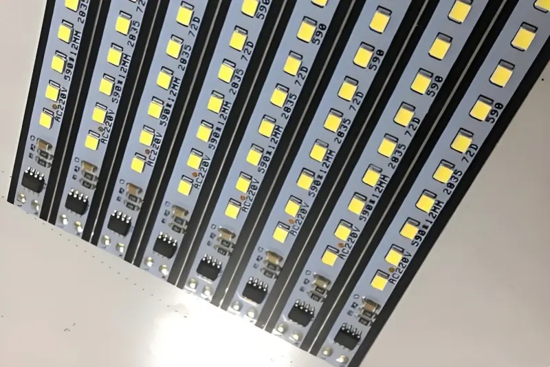
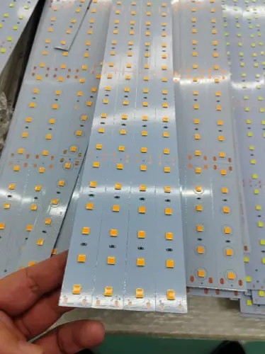
The typical structure consists of three primary layers: a copper circuit layer where components mount, a thermally conductive dielectric that provides electrical isolation while allowing heat transfer, and an aluminum base plate that acts as the primary heat spreader. The aluminum substrate typically ranges from 1-3mm thick, providing mechanical rigidity alongside thermal performance.
The dielectric layer is where aluminum PCB design gets interesting. This specialized material must simultaneously insulate electrically—preventing shorts to the metal core—while conducting heat efficiently. Modern dielectric materials achieve thermal conductivity values between 1-8 W/mK, dramatically outperforming standard FR-4’s 0.3 W/mK.
Thermal vias enhance this structure further by creating vertical heat pathways through the copper and dielectric layers, channeling concentrated heat directly to the aluminum base. This layered approach creates what engineers call a “thermal highway”—a low-resistance path that pulls heat away from critical components before temperatures climb into dangerous territory.
Key Design Principles for Optimizing Heat Dissipation
Effective heat dissipation in aluminum PCBs requires strategic design decisions that maximize thermal transfer paths. The most critical principle involves minimizing the thermal resistance between heat-generating components and the aluminum base layer—this means keeping copper traces thick (2-3 oz copper is common) and placing high-power components directly over areas with maximum thermal contact.
Component placement matters enormously. Position heat-generating parts like power MOSFETs, voltage regulators, and LEDs with sufficient spacing to prevent thermal interference. A practical approach is maintaining at least 10mm between high-power components when possible, allowing heat to spread laterally through the dielectric before transferring to the aluminum substrate. Strategic thermal via placement further enhances vertical heat transfer in multi-layer designs. The dielectric layer thickness directly impacts thermal performance—thinner layers (typically 3-6 mils) provide better conductivity but reduce electrical isolation. Balance this trade-off by selecting dielectric materials rated for your voltage requirements while maintaining thermal conductivity above 2 W/m·K. What typically happens is engineers over-specify dielectric thickness for safety margins, inadvertently creating thermal bottlenecks.
Design your aluminum PCB with the entire thermal pathway in mind—from component junction to ambient air.
Comparison of Heat Dissipation Techniques
Thermal management strategies for power electronics extend beyond material selection alone. While aluminum PCBs offer inherent advantages, designers must evaluate multiple heat dissipation approaches to optimize performance.
Passive cooling through aluminum substrates typically handles 2-5W/cm² heat density effectively without additional components. This approach works well for automotive lighting and LED applications where space constraints limit active solutions. However, high-power electronics demanding greater thermal capacity often require supplementary techniques.
Active cooling systems—fans or liquid cooling—can extend thermal capacity beyond 10W/cm² but introduce mechanical complexity and potential failure points. A common pattern is combining aluminum PCBs with finned heatsinks, which increases surface area by 300-400% compared to flat boards. This hybrid approach balances cost against performance requirements.
The critical differentiator remains thermal resistance. Standard FR-4 boards measure 20-30°C/W, while aluminum PCBs achieve 1-2°C/W—a tenfold improvement. For power converters and motor controllers, this gap determines whether passive cooling suffices or active systems become necessary.
Design Considerations for Aluminum PCBs in Power Electronics
إلكترونيات الطاقة applications demand careful attention to electrical isolation alongside thermal performance. The dielectric layer in aluminum PCBs serves a dual purpose: it must efficiently transfer heat while maintaining high voltage breakdown resistance—typically ranging from 2,000V to 3,000V depending on the application requirements.
Component placement becomes particularly critical in high-power designs. Position heat-generating devices like MOSFETs, IGBTs, and voltage regulators directly over the aluminum base to minimize thermal resistance paths. Thermal analysis tools can predict hotspot formation before fabrication, allowing designers to adjust layouts proactively rather than discovering issues during prototyping. Copper trace thickness requires recalculation for aluminum substrates. While standard PCBs typically use 1-2 oz copper, power electronics often benefit from 3-4 oz copper layers to handle higher current densities. However, thicker copper increases manufacturing complexity and cost—design teams must balance current-carrying capacity against thermal performance needs when specifying trace specifications.
Surface mount assembly considerations also shift with aluminum substrates, as the metal base alters reflow profiles and may require adjusted soldering parameters to prevent warping or delamination during manufacturing.
Best Practices for Aluminum PCB Layout
Component placement directly impacts thermal performance in aluminum PCB designs. Position high-power components where they can transfer heat most efficiently to the aluminum base layer, typically avoiding board edges where thermal paths become constrained. A common pattern is clustering heat-generating components in the center of the board, allowing heat to spread radially outward.
Trace routing requires special attention to current capacity aluminum PCBs can handle. Wider traces reduce electrical resistance and lower heat generation, but they also improve thermal coupling to the aluminum substrate. Advanced thermal management approaches recommend maintaining minimum 0.5mm spacing between high-current traces to prevent thermal crosstalk while maximizing copper coverage for heat spreading.
Via placement enhances thermal transfer where FR-4 layers meet aluminum substrates in hybrid designs. However, avoid overusing vias near sensitive components—excessive vias can create unintended thermal paths that concentrate heat in localized areas. The balance lies in strategic placement where thermal conductivity benefits outweigh potential hot-spot risks, setting up considerations for different power level scenarios.
Example Scenarios: Designing for Different Power Levels
Power level requirements fundamentally shape aluminum PCB design decisions. A low-power LED lighting application handling 5-10W typically functions well with a standard 1.5mm aluminum substrate and basic thermal conductivity ratings around 1.0-2.0 W/m·K in the dielectric layer. Component spacing can be tighter, and the aluminum base provides sufficient heat spreading without additional thermal management features.
Mid-range power electronics (50-100W) demand more strategic approaches. Motor controllers and power supplies in this category benefit from thicker copper layers (3-4oz) and higher thermal conductivity dielectrics (2.0-3.0 W/m·K). Designers should position high-dissipation components near board edges where heat can escape more readily, and consider increasing board thickness to 2.0-2.5mm for enhanced heat spreading.
High-power applications exceeding 200W require aggressive thermal optimization. These designs often specify premium dielectric materials with thermal conductivity above 3.0 W/m·K, maximum copper weights (5-6oz), and dedicated thermal vias connecting component pads directly to the aluminum base. Board thickness may reach 3.0mm, and designs typically incorporate mounting provisions that ensure direct mechanical contact between the aluminum substrate and external heatsinks.
Limitations and Considerations in Aluminum PCB Design
Despite their thermal advantages, aluminum PCBs present constraints that designers must navigate carefully. The single-layer construction inherent to most aluminum PCBs limits routing flexibility compared to traditional multi-layer boards. This restriction becomes particularly challenging in dense circuit layouts where component count exceeds available routing space.
Cost considerations often surprise first-time aluminum PCB users. According to Aluminum PCB Boards — an engineer’s practical guide, material and manufacturing expenses typically run 2-3x higher than standard FR-4 boards due to specialized dielectric layers and processing requirements. This premium makes aluminum PCBs economically viable primarily when thermal performance justifies the investment.
High voltage aluminum PCB applications introduce additional complexity. The dielectric layer must provide adequate electrical isolation while maintaining thermal conductivity—a balancing act that requires careful material selection. Typical dielectric breakdown voltages range from 2-3 kV, sufficient for most power electronics but potentially limiting for higher voltage systems.
Mechanical considerations also matter. While aluminum provides structural rigidity, it complicates mounting scenarios requiring board flexibility. The metal base also conducts electricity, demanding insulated standoffs and careful mechanical design to prevent short circuits through mounting hardware. These practical constraints shape whether aluminum remains the optimal substrate choice.
الوجبات الرئيسية
Aluminum PCB design for power electronics centers on balancing thermal performance with practical constraints. The substrate’s thermal conductivity—typically ranging from 1-8 W/mK—directly impacts heat transfer efficiency, with higher values enabling tighter component spacing and reduced thermal resistance. سُمك النحاس selection proves equally critical, as 2-3 oz copper effectively handles high-current applications while maintaining mechanical stability during thermal cycling.
Single-layer limitations demand strategic component placement, particularly for heat-generating devices like MOSFETs and power diodes. Position these elements directly over the aluminum base for optimal thermal coupling, maintaining adequate spacing to prevent thermal interference. The dielectric layer thickness—usually 75-150μm—represents a crucial tradeoff: thinner improves heat transfer but reduces electrical isolation.
When aluminum PCBs fall short for complex power electronics, thermal vias and multi-layer designs with dedicated heat spreaders offer enhanced versatility. However, for high-power LED arrays, automotive modules, and power supplies under 100W, aluminum substrates deliver unmatched cost-effectiveness and reliability. Success hinges on early thermal simulation, realistic power budgets, and manufacturer collaboration to validate design choices before production.
Design Considerations for Aluminum Pcbs in Power
Power electronics introduce electrical safety requirements that complicate aluminum substrate design. The conductive base plate creates unique challenges for creepage clearance aluminum PCB layouts, where designers must maintain adequate spacing between high-voltage traces and the grounded aluminum core. Aluminum PCB Boards — an engineer’s practical guide notes this necessitates thicker dielectric layers than FR-4 equivalents—often 4-6 mils minimum—compromising thermal conductivity.
Component placement becomes particularly critical in power applications. Position high-dissipation devices directly above areas with optimal heat extraction paths, avoiding regions near mounting holes where thermal resistance increases. The Role of Aluminum PCBs in Power Electronics emphasizes that trace width calculations must account for both current-carrying capacity and thermal spreading—wider copper features distribute heat more effectively but consume limited single-layer real estate.
Dielectric breakdown voltage ratings determine maximum operating voltages, typically ranging from 2-4 kV for standard materials. What typically happens is engineers specify higher-voltage dielectrics for mains-connected circuits, accepting the thermal trade-off for regulatory compliance and long-term reliability.
Final Thoughts on Aluminum PCB Design
Successful metal core PCB implementation comes down to understanding the fundamental trade-offs between thermal performance, electrical isolation, and manufacturing constraints. The most effective designs don’t simply maximize thermal conductivity—they match substrate properties to actual power dissipation patterns while maintaining reasonable production costs.
The thermal benefits only matter if your design accounts for the limitations. Designs that ignore electrical clearance requirements or assume unlimited vias typically fail during thermal testing. The substrate choice should follow your thermal analysis, not precede it.
Start with conservative assumptions: model worst-case power dissipation, verify dielectric breakdown margins exceed 2× operating voltage, and prototype with standard 2 W/m·K substrates before specifying exotic materials. Testing reveals that 70% of thermal improvements come from optimized component placement rather than substrate upgrades.
Your next step: Calculate your actual power density per square centimeter. If it exceeds 5W/cm², aluminum substrates deserve serious consideration. Below that threshold, enhanced FR-4 constructions often provide better value without introducing grounding complications.

