Abstract
This paper explains the classification, material choice, technology trends, design rules, and processing standards for printed circuit boards (PCBs) used in communication products. It is for PCB designers and process engineers to use.
Purpose and Function of Printed Circuit Boards
Electronic communication systems use many printed circuit boards. These boards are the functional parts of hardware. They are like organs in a body. Boards on a system or a terminal carry circuits. They form the skeleton, the wiring, and the pathways for power and signals.
Types of Printed Circuit Boards
Classify PCBs by use and by technology. By structure and by function, there are single-sided boards, double-sided boards, and multilayer boards.
PCB Substrate Material Types and Properties
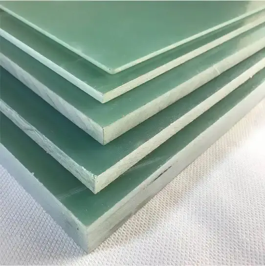
Substrate materials divide into rigid substrates and flexible substrates. Rigid PCBs include copper-clad phenolic paper laminates, copper-clad epoxy paper laminates, and copper-clad epoxy glass-fiber laminates. These use phenolic resin or epoxy resin as the binder. They use paper or alkali-free glass cloth as the reinforcement. After one or two sides are clad with copper foil, they become electrical insulating laminates.
The properties of these substrate materials should meet widely recognized international standards such as IPC-4101 (Specification for Base Materials for Rigid and Multilayer Printed Boards) and relevant IEC publications; flame-retardancy is commonly verified by UL 94 vertical burn ratings, and the NEMA LI-1 / FR-4 designation is used internationally to identify glass-epoxy laminates. When specifying materials for global manufacture, refer to IPC “slash-sheets” (exact resin/fabric/copper combinations) or IEC identifiers so suppliers and fabricators worldwide can locate equivalent stocked products and ensure consistent performance.
3.1 Copper-Clad Epoxy Glass-Fiber Laminate
This laminate uses epoxy resin as the binder and glass fiber cloth as the reinforcement. It has better mechanical strength, dimensional stability, and impact resistance than paper laminates. The dielectric constant ε for FR4 and FR5 is between 4.3 and 4.9. Their electrical properties are good. They can work at higher temperatures. FR4 works to 130℃, FR5 to 170℃. They are less affected by humidity. This is why they are widely used in communication equipment.
3.2 Epoxy Glass-Fiber Bonding Sheets for Multilayer Boards (Prepreg)
These are glass cloth materials pre-impregnated with B-stage epoxy resin. Use them to make multilayer boards. They bond separate طبقة واحدة or double-layer conductive pattern boards together. After lamination, they act as dielectric insulation layers. They are made by pre-impregnating alkali-free glass cloth with epoxy. The resin is cured to the B stage. After final pressing and forming, the epoxy fully cures. The result is a rigid multilayer PCB.
3.3 Self-Extinguishing (Flame-Retardant) Copper-Clad Laminates
These materials have the same basic properties as other copper-clad laminates. They also resist fire. They reduce the risk of ignition from an overheated component. They also limit small fire spread. Use them where fire safety is needed.
3.4 Copper-Clad PTFE (Teflon) Glass-Fiber Boards
Copper-clad PTFE boards use PTFE (Teflon) as the binder and glass fiber as reinforcement. Their dielectric properties are excellent. They have low dielectric loss and a tangent loss (tgδ) on the order of 10⁻³. Their dielectric constant range is wide. You can choose a variety of base materials to meet needs. They resist high temperature and moisture. They have good chemical stability. They work across a wide temperature range. These features make them ideal for high-frequency and microwave communication PCBs.
But PTFE boards cost more. They are less rigid. Copper foil adhesion strength is lower. This makes high-count multilayer boards hard to build. Common PTFE PCB base materials come from Rogers, Taconic, Arlon, Metclad, and GIL.
3.5 Copper-Clad Metal-Core PCBs
Also called metal-core PCBs, these use metal plates of various thicknesses, usually aluminum, instead of glass-fiber reinforced materials. After special treatment, the metal surface is covered with a dielectric layer. The dielectric has low thermal resistance, high insulation, and strong bonding. Then copper foil of required thickness is bonded to the dielectric surface.
Metal-core PCBs are used for high-density assembly and high power density. Use them for power circuits with high dissipation. Their advantages are good heat dissipation and good dimensional stability. The metal base also offers shielding. Current products use materials from suppliers like Bergquist and research institutes such as Institute 51 of the Ministry of Information Industry.
3.6 Flexible PCB Substrate Materials
ثنائي الفينيل متعدد الكلور المرن substrates are made by bonding copper foil to thin plastic film. Common plastic film base materials are:

(1) Polyester film. Work temperature is 80℃ to 130℃. It has a low melting point. It softens and deforms at soldering temperatures.
(2) Polyimide film. It has good flexibility. Remove absorbed moisture by heat treatment before soldering. After drying, it can be soldered safely. General adhesive-type polyimide film can work continuously at 150℃. Polyimide material that uses FEP as an intermediate film and a special fusion adhesive can work at 250℃.
(3) Fluorinated ethylene propylene film (FEP). Often used with polyimide and glass cloth. It has good flexibility. It has higher resistance to moisture, acid, and solvents.
Main Trends in PCB Technology Development
The main trend for PCB development is higher density. Ways to reach high density are fine lines, small via holes, more layers, blind vias, and buried vias. The common process for high density (HDI) is buildup multilayer (BUM) technology.
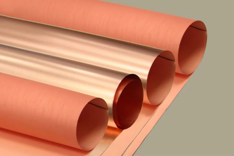
Main Performance Indexes and Copper Foil Thickness Selection for Copper-Clad Epoxy Glass-Fiber Laminate
Besides thickness and copper foil thickness, laminates have other properties. These include peel strength, warpage, dielectric strength, insulation resistance, dielectric constant, dielectric loss tangent, heat shock resistance, moisture absorption, and flame retardance. Technical requirements for copper-clad epoxy glass-fiber laminates should meet GB/T4725.
Copper foil thickness has a large effect on the precision of printed conductors and the minimum conductor width in manufacturing. The general rule is: the thicker the copper, the larger the etch undercut. The printed conductor narrows more. When the conductor width becomes too small, it cannot be produced. So when you set the PCB minimum conductor width, consider copper thickness besides current, routing density, and other rules.
Data show that for 35 μm copper foil, conductor width should be greater than 0.15 mm. For 18 μm copper foil, conductor width should be greater than 0.1 mm.
PCB Outline Choice, Thickness, and Single-Board Size
6.1 Single-Board Outline Choice
PCBs usually use a rectangle with similar length and width. Avoid odd-shaped boards. For ease of line transfer and insertion into racks, corners may use small round arcs or chamfers.
Very small boards (for example, boards smaller than 100 mm × 100 mm) should be panelized. When several board types for one product have the same layer count, same thickness and dielectric layers, same copper thickness, and the same quantity, combine them into a single panel.
6.2 PCB Thickness
Choose board thickness by function, component mass, matching connector specs, board size, and mechanical load. For large boards that deform easily, add ribs or frames to strengthen them.
For boards under 300 mm × 250 mm, a general thickness of 1.6 mm is common. Backplanes and larger single boards should be thicker than 2 mm. But press capacity limits processing. Thickness generally should be under 4 mm.
6.3 PCB External Dimension Series
For PCBs not placed in a rack, refer to GB9315 for board dimension series. In cabinets, plug-in PCBs with edge connectors are common.
Notes and Simple Advice
- Choose materials that meet standards and that the maker can stock. This reduces delay.
- For high-frequency boards, use PTFE-based material when you need low loss and stable dielectric constant. Check cost and build limits.
- For heat-critical power boards, consider metal-core boards for better heat spread.
- For flexible circuits, pick polyimide or FEP types as needed for soldering and temperature. Dry the materials if they absorb moisture.
- For HDI designs, plan vias and layer build early. Use buildup methods when you need many blind or buried vias.
- For manufacturing, list critical items in drawings: final thickness, layer pair core thickness, copper weight per layer when needed, which layers are signal and which are planes, and target impedance for critical nets. Add a note that prepreg placement will be set by the manufacturer to meet impedance and total thickness, unless exact prepreg sheets are required and the designer can specify them with confidence.