


Background
The resin-filled via process is used more and more in PCB making. It is common in boards with many layers and in high-precision PCBs. Resin filling can solve many problems that solder-mask plugging or lamination filler resins cannot solve. At the same time, the resins used in this process have special properties. Those properties bring many hard points in the board making steps.
Definition
Resin plugging means using resin to fill buried vias on inner layers, then doing lamination. This method is widely used in high-frequency boards and HDI boards. There are two main types: traditional screen-printed resin plugging and vacuum resin plugging. Most products use the traditional screen-print resin method. This is also the most common method in the industry.
What is a “plugged via” on a PCB?
Via function and industry need
A via (plated through hole, PTH) connects different layers on a board. The growth of the electronics industry pushes PCB technology forward. It also raises the need for better board making and surface mount work. The plugged via process appears to meet these needs. Plugging must meet these rules:
The via must have copper inside. The via can be filled or not filled under the solder mask.
The via must have solder (tin-lead) inside with a certain thickness (for example 4 μm). Solder mask ink must not enter the hole and cause trapped solder beads.
The via must be covered by solder mask so that light cannot pass. The hole must not have solder rings or solder beads. The filled hole must be flat.
As electronic products become lighter, thinner, shorter, and smaller, PCBs also move to high density and higher difficulty. This brings many SMT i BGA boards. When customers assemble parts, they often ask for plugged vias. Plugging serves five main purposes:
To stop solder from passing through the via during wave solder and shorting the part side. This is key when a via is placed on a BGA pad. Then plugging is done first, then gold plating, to make BGA soldering easier.
To avoid flux residue left inside the via.
To allow vacuum pick-and-place or vacuum test steps after surface mount and assembly. A sealed top is needed for vacuum to work.
To stop paste from flowing into the via and cause weak solder joints or poor placement.
To stop solder balls from popping out during wave solder and causing shorts.
Advantages of Resin-Filled Vias
On multi-layer boards with BGA, resin plugging can reduce the gap between vias. This helps routing and trace layout.
For buried vias in inner HDI layers, resin fill helps balance the thickness control of the prepreg during lamination and the resin fill design of the buried via.
For thick boards with large through holes, resin filling improves product reliability.
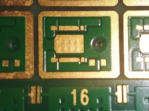
Resin-filled vias are often used because of BGA parts. In traditional BGA, a via may route from pad to the back side. If the BGA is dense and the via cannot route out, you can drill a via in the pad and route to another layer. Then you fill the hole with resin and plate copper to make it a pad. This is called the VIP process (via in pad). If you drill a via in the pad and do not use resin fill, solder may leak and cause a back-side short or a poor joint on the pad.
Process Flow for Resin-Filled Vias
General resin-filled via process:
Drill holes.
Plate through holes with copper.
Fill holes with resin and bake.
Grind or mill flat (planarize).
After grinding, the resin part has no copper. Then a new copper plating step is needed to turn the filled area into a pad. This plating step is done before the normal drilling for other holes. In short, handle the vias that will be filled first, then drill other holes and follow the normal flow.
Below are some key steps and stations you may see in a factory:
VIP plating and panel grinding
Aluminum sheet screen / pads
Mount aluminum sheet and pad board for board making
Test print film alignment and mix ink
Trial printing
NG line self-check, OK for batch production, section curing
IPQC sampling
Ceramic panel grinding
Outer layer and photo film conditions
If the outer layer work meets the negative film limits and the PTH aspect ratio ≤ 6:1:
Conditions to meet: line width and gap are large enough, maximum PTH hole is smaller than the dry film seal limit, board thickness is less than the dry film max thickness, and there are no special requirements like local electroless gold, nickel-gold boards, half-hole boards, plug-in boards, no annular PTH, or PTH slot holes.
Standard inner layer making → lamination → brown oxide → laser drilling → de-brown → outer drilling → immersion copper → panel fill electroplating → cross-section analysis → outer pattern → outer acidic etch → outer AOI → follow normal flow.
If outer layer meets negative film but PTH aspect ratio > 6:1:
When aspect ratio > 6:1, full panel via fill plating cannot reach the required copper thickness in the via. After panel fill plating, a second full-board electroplating is needed to increase via copper thickness. Flow:
inner layer making → lamination → brown oxide → laser drilling → de-brown → outer drilling → immersion copper → panel fill electroplating → full-panel electroplate → cross-section analysis → outer pattern → outer acidic etch → follow normal flow.
If outer layer does NOT meet negative film, but line width/gap ≥ a and outer PTH aspect ratio ≤ 6:1:
inner layer making → lamination → brown oxide → laser drilling → de-brown → outer drilling → immersion copper → panel fill electroplating → cross-section analysis → outer pattern → outer electroplate → outer alkaline etch → outer AOI → follow normal flow.
If outer layer does NOT meet negative film, or line width/gap < a, or line width/gap ≥ a but PTH aspect ratio > 6:1:
inner layer making → lamination → brown oxide → laser drilling → de-brown → immersion copper → panel fill electroplating → cross-section analysis → copper reduction → outer drilling → immersion copper → full-panel electroplate → outer pattern → pattern electroplate → outer alkaline etch → outer AOI → follow normal flow.
Cross-Section and Quality Notes
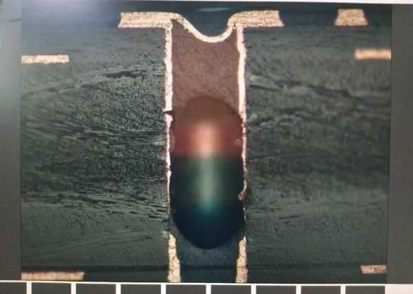
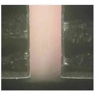
Resin plug cross-section
From cross-section analysis, a good resin-ink plugged via shows full resin fill. The resin fills the hole to 100%. The resin surface at top and bottom is evenly slightly convex. After this, ceramic panel grinding is used to level the surface.
Filling quality and checks
The resin fill must be full with no voids.
The plug surface must be flat after grinding.
The via copper must meet thickness rules after final electroplating.
Check for trapped solder balls or solder rings. These must not exist.
Check that the plug is not light-transmitting after mask or cover.
Practical Notes and Best Practices
For VIP (via in pad) work, do the via filling and make the pad on those spots before normal drilling and other steps. This prevents mis-process and helps final plating quality.
When a board has many buried or blind vias, plan the pad and fill steps to keep lamination thickness stable.
Use proper resin type and curing profile. Resin choice affects flow, cure, and grinding behavior.
Use IPQC sampling and cross-section checks after the panel fill step to confirm copper inside the via and resin fill quality.
Use AOI and other final tests to ensure no solder mask or paste issues remain.
Sažetak
Resin-filled via is a key process for modern HDI and BGA boards. It helps routing, improves reliability, and protects against solder defects. It requires careful control of drilling, plating, resin filling, baking, and grinding. When planned well, resin plugging lets you use VIP designs and meet tight BGA pad needs.