
Osazení desek plošných spojů
File Guide
See how your board data, parts list and placement information work together — and let us help fill in the gaps.
Send the information already available for your project. FLJ PCB’s engineers will review it and discuss any additional data that would help with the quotation or assembly preparation.

What information describes an assembled board?
A PCB assembly combines a bare board with electronic components. The fabrication files describe the board; the bill of materials (BOM) identifies the parts; placement data and drawings explain where and how the parts are fitted.
These documents often come from the same CAD project, but each answers a different question. You can begin an enquiry with the information you have. We’ll review it together and explain which additional outputs would be useful.
| Document | What it tells the assembly team |
|---|---|
| PCB or fabrication data | The board layout, shape and assembled sides |
| BOM | The components and quantities for the build |
| Placement file / CPL | Component positions, rotation and board side |
| Assembly drawing | Reference labels, polarity and special assembly details |
| Test or programming notes | How the finished product should be checked or programmed |
What is a pick-and-place file?
A pick-and-place file lists component locations for assembly preparation. It is also called a centroid file, component placement list (CPL), position file or XY file. A row typically contains a reference such as U1, X and Y coordinates, a rotation angle and the board side.
Think of it as the location information that accompanies the parts list. The BOM tells us which device U1 is; the placement output shows where U1 belongs. CAD tools can export this data as CSV, text or a position-file format.
The coordinate origin, units and angle convention depend on the export settings. Our engineers can compare the placement data with the drawing or board view and ask about any unclear orientation during review.

How the BOM and drawing help
The BOM is your parts list for the assembled product. Manufacturer and part number help identify the component, while reference designators connect it to positions on the board. The BOM and component guide explains these fields and sourcing choices in more detail.
An assembly drawing gives a readable view of the board. Reference labels and polarity marks help explain connectors, diodes, IC pin 1 and any other orientation-sensitive parts. Photos can provide useful additional context for a sample or existing build.
Some products share one bare PCB but fit different parts. These are assembly variants. A note about the version you want helps us discuss fitted parts, optional positions and items marked DNP — do not populate.
Paste layers and stencil preparation
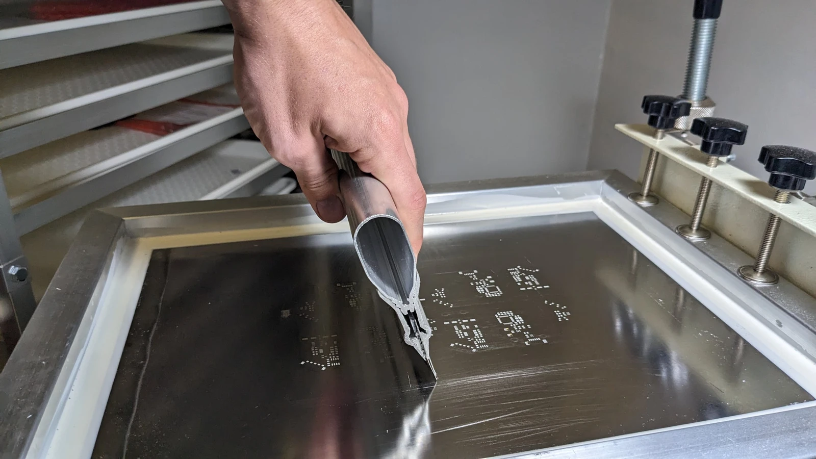
Solder paste is applied to the pads before SMT components are placed. The paste-layer output shows the intended openings used in stencil preparation. Solder mask is a different layer: it describes where the board’s protective coating exposes the surface.
If you have paste outputs or an existing stencil drawing, include them with the board data. Fine-pitch parts, exposed thermal pads or special assembly instructions are useful topics to discuss with our engineers.
For a new design, we can review the available outputs and talk through stencil preparation as part of assembly planning. You can start by sharing the board package rather than working out every process detail yourself.
Single boards, panels and through-hole parts
Boards may be assembled individually or as a panel containing several circuits. If you have a panel drawing or a photo of supplied boards, it helps us understand the arrangement. We can discuss panel preparation when the design is still a single board.
Through-hole parts may be fitted using a different process from SMT components. A drawing or note can help explain connector height, lead treatment, hardware or a particular mounting arrangement. Include the details you already know and we’ll follow up on the rest.
Tell us how the product should work
Pro programming, the firmware file and a note about the device or interface give us a starting point. For testing, describe the functions you would like checked, such as a communication interface, sensor output or power rail.
If you already have a test procedure, fixture or known-good sample, we can discuss how it fits into the assembly project. If you are still developing the test approach, explain the intended behavior and we can review the preparation needed.
Testing and programming are easier to plan when they are part of the early conversation, even if the instructions are still being developed.
Your questions, answered
I have Gerber files and a BOM, but no placement file. Can I enquire?
Yes. Send the available data and tell us which CAD tool was used if you know it. Our engineers can review the package and discuss the placement information or export that would help.
Can a board photo help explain the assembly?
Yes. Photos are useful for identifying orientation, connectors and special mounting details, especially for an existing product. We’ll look at them alongside the available design data.
What if the BOM is still being revised?
Let us know which version is current and which parts are still under consideration. We can discuss the project and sourcing while those decisions are being finalized.
Can I send an updated file after the enquiry?
Yes. Tell us what changed so we can review the update with you and discuss any effect on the quotation or order.
Let’s review your assembly project
Share the board files, parts list and any drawings or notes already available. We’ll help you connect the information and work through the next steps.
E-mail [email protected] with your files or question. Our team will review the information and follow up with you about the next step.
Explore the technical details: Ucamco Gerber documentation · KiCad PCB Editor documentation. Software examples illustrate the tools; your design may use a different workflow.