
6-Layer PCB Manufacturing
Build a compact controller, interface board or connected device around six layers of copper. FLJ manufactures the bare board with internal routing, ground and power planes arranged for your circuit, from the first prototype to production batches.
Specify the laminate, finished thickness, inner and outer copper, surface finish and interconnections. Bring a completed layout or develop the fabrication stackup with FLJ while the design takes shape.
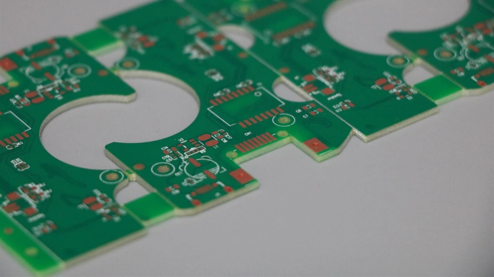
6-Layer PCB Configurations for Your Circuit
Six copper layers create room for more than additional traces. An internal power layer can free surface space around connectors and ICs. Two ground layers can place references beside several routing layers. Extra internal routing can relieve congestion when a four-layer design runs out of usable channels.
Consider a controller with connectors around the board edge and several supply rails feeding its ICs. Moving power distribution onto an internal layer releases surface area for component escape and connector routes. Allocating four layers to signals offers more routing space instead, but supply traces or copper regions must then occupy part of that space. The extra copper is useful when its assigned job resolves the actual bottleneck.
Three signal layers, two ground layers and a power layer
- L1SignalRouting
- L2GroundReference
- L3SignalRouting
- L4PowerSupply
- L5GroundReference
- L6SignalRouting
An internal power plane
Dedicated power distribution with ground beside each signal layer in this arrangement. The inner signal layer also couples to the power layer on its other side.
Four signal layers and two ground layers
- L1SignalRouting
- L2GroundReference
- L3SignalRouting
- L4SignalRouting
- L5GroundReference
- L6SignalRouting
An extra signal layer
Additional routing resources, with power carried in traces or copper regions. The two central signal layers need attention to their separation and mutual coupling.
These are electrical allocations, rather than material schedules. Signal and power regions may share a layer, and the final reference relationships depend on the actual copper layout and dielectric spacing.
Give the extra layers a defined job
Six layers are useful when extra routing or a different plane arrangement addresses a real layout constraint. Dense component placement, several supply rails and mixed signal functions may each favor a different distribution. A board that already routes cleanly in four layers may gain little from adding copper layers alone.
Package escape remains a local problem. The pad pattern, via position and diameter, available trace space and reference connections determine how signals leave an IC. More layers create destinations for those routes; they do not create space between pads. If six layers still cannot accommodate the escape and reference needs, compare an eight-layer construction or a different interconnect approach.
Stackup Construction and Board Thickness
A six-layer stackup contains six copper layers separated by five dielectric regions. In one conventional foil build, two double-sided cores form the four inner copper layers. Prepreg bonds the cores to each other and to the outer copper foils. The outer circuits are then processed as part of the plated board.
Core and prepreg describe materials; signal, ground and power describe electrical functions. Assigning a ground layer does not determine its core thickness, and choosing a prepreg cloth does not by itself define the final pressed dielectric gap.

From a layer sequence to a physical construction
For the three-signal-layer example, the top signal is next to L2 ground, the internal signal on L3 is next to that same ground layer, and the bottom signal is next to L5 ground. L4 power and L5 ground form an adjacent plane pair. Changing the dielectric gaps changes how strongly those neighboring conductors couple.
The illustration separates those electrical roles from the core and bonding regions. It represents one construction, rather than a standard thickness recipe. Other core and foil arrangements can produce six copper layers with different local geometry.
Five dielectric regions do not mean five sheets of prepreg. A bonding region may contain more than one ply, while a cured core already separates two copper layers. Resin content, adjacent copper pattern and pressing conditions affect the resulting bonding thickness. The finished construction brings those material choices together with the required electrical spacing.
Use the thickness that belongs to the question
Finished board thickness sets the mechanical envelope for the enclosure, mounting hardware and connector engagement. Signal-to-reference spacing is a local dimension inside that envelope. Two boards with the same finished thickness can place a signal very differently relative to its reference plane.
Impedance routing depends on that local spacing together with material properties, finished conductor width and thickness, and differential-pair spacing where relevant. Etching and plating affect the conductor geometry; resin flow and curing affect the bonding dielectric. Calculations should therefore describe the fabricated construction rather than substitute the initial material thicknesses.
The stackup specification connects these requirements: layer sequence, laminate and prepreg construction, pressed dielectric values and finished copper. It provides the common geometry for layout and fabrication.
Laminate, Copper and Surface-Finish Options
The material and copper build turn the layer arrangement into a board suited to its electrical path and assembly conditions. FLJ fabricates six-layer boards with the selected laminate system, internal and external copper, solder mask and finish.
| Board option | Selection considerations |
|---|---|
| Laminate and bonding system | Material grade, dielectric properties at relevant conditions, thermal behavior and compatibility through lamination and assembly. |
| Finished thickness | Mechanical fit together with the dielectric spacing needed by the electrical design. |
| Inner and outer copper | Current distribution, conductor geometry, feature size and the copper build after processing. |
| Surface finish | Solderable pads, component assembly and any separately specified contact areas. |
| Hole and via construction | Connected layers, component leads, routing density and the manufacturing route. |
| Controlled impedance | Signal and reference layers, target and tolerance, finished geometry and coupon requirements. |
Choose the material system, not a single label
FR-4 covers a family of glass-reinforced resin materials. Glass construction, resin content, frequency and the measurement method influence the dielectric values used in a circuit model. Tg describes the glass transition; it does not alone specify insertion loss or a continuous operating-temperature rating.
For a long high-speed channel, dielectric loss and copper surface roughness can matter alongside routing geometry. A short connection may justify a different material choice from a long connector-to-connector path. Material selection should follow the electrical channel and thermal exposure, rather than upgrade every six-layer board to the same laminate.
Specify copper where the circuit uses it
Inner copper is formed into the internal circuits before lamination. Outer copper is processed with the plated board, so starting foil and finished conductor thickness are different specifications. Power distribution may justify heavier copper, while dense routing also needs suitable conductor width, spacing and etched geometry.
Copper distribution matters mechanically as well as electrically. A balanced construction considers the material build and copper pattern across the stack, rather than assuming that an even layer count guarantees flatness.
Match the finish to the exposed feature
The surface finish protects exposed copper and prepares the required interface. Solder pads and wear contacts have different tasks. ENIG, HASL and OSP are examples of solderable finish options; connector contacts may need a separately specified contact finish. For dense surface-mount pads, surface geometry and compatibility with the assembly process matter; a connector wear surface has a different service requirement. Identify each finish and its physical region in the fabrication data, especially where solder pads and contact fingers share a board.
Interconnects and Manufacturing Quality
The layer stack becomes an electrical circuit through registered copper patterns and plated connections. FLJ forms and optically checks the internal circuits before they are enclosed by lamination, aligns the layers during lay-up, and processes the external circuits and holes to complete the board.
Connect the required layers
In a conventional plated-through-hole construction, holes are drilled through the laminated panel. Hole-wall preparation and copper deposition create a conductive connection to the designated lands. Clearance openings isolate the barrel from copper layers that must not connect to that net.
Blind or buried vias, filled via-in-pad structures and backdrilling address different routing or assembly needs. Their layer spans, depths and process sequence affect fabrication. A mechanically drilled hole is larger before hole-wall copper is added; the finished hole size is the remaining opening. Component fit and drill geometry therefore use different dimensions. For a depth-to-drill assessment, the relevant inputs are the actual drilled depth and the drill diameter before plating. A six-layer board does not automatically require those features: ordinary through vias may provide the needed interconnections, while finer escape or stub control can call for a different route.
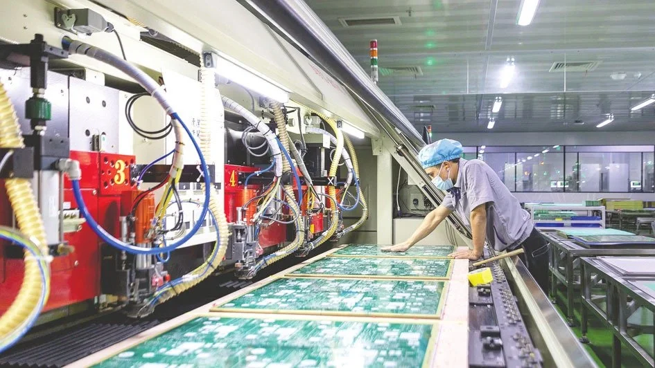
Check the structure and the circuit
| Check | What it examines |
|---|---|
| Inner-layer optical inspection | Circuit features while the inner copper remains accessible, before lamination. |
| Registration and dimensional inspection | Alignment, hole and feature locations, outline and finished dimensions. |
| Electrical continuity and isolation | Whether the fabricated nets connect and remain separated as intended. |
| Controlled-impedance coupon testing | The electrical behavior of the defined representative test structures. |
| Relevant cross-section inspection | Selected internal dimensions and hole-wall features visible in the prepared sample. |
Each check answers a different manufacturing question. Continuity testing checks the connection network; it does not measure channel loss or the finished product’s emissions. Prototype and production requirements determine the additional measurements and records needed for the build.
What Affects 6-Layer PCB Cost?
Layer count is only the starting point for a quotation. Laminate choice, finished size, copper, drill features, surface finish and testing determine the work needed to manufacture the board. A conventional through-hole six-layer board and a six-layer design with special interconnects can have substantially different manufacturing routes. Connections formed before the full stack is enclosed may add separate processing and inspection stages. Filling, capping or a backdrill operation adds different work again; the cost follows the construction rather than a fixed price multiplier for six layers.
Panel use and order quantity
Fabrication uses working panels that also need room for process features. Board outline, spacing, rails and test coupons affect how many useful circuits fit. A small board can still use panel area inefficiently if its shape or array arrangement leaves unusable space.
Engineering preparation and tooling are shared across a batch. Increasing quantity spreads those costs across more boards, while material and processing costs remain. For a repeat order, an unchanged construction makes comparison more useful than comparing layer count alone.
Compare the same manufactured product
Compare quotations against the same material grade, thickness, inner and outer copper, finish, hole construction and inspection scope. Identify setup charges separately from repeat fabrication, and keep component sourcing and assembly distinct from the bare-board price.
Special material, a tighter feature set or additional coupon requirements can explain a price difference that the words “six-layer PCB” conceal. The useful comparison is the complete board and its delivery scope.
Start Your 6-Layer PCB Build
For a design ready to fabricate, send the fabrication artwork, drill data, board dimensions, quantity and available stackup information. Include controlled-impedance requirements and special finish or hole details where they apply. FLJ uses the drawing and layer definition to prepare the manufacturing build.
If the construction is still being developed, start with the board envelope, circuit requirements and the decisions still open. Material and stackup selection can progress alongside the layout. Available drawings and a clear description of the intended use are enough to begin that conversation; open choices can be identified in the enquiry.
Assembly is available alongside bare-board manufacturing. Add the BOM and placement information when the order includes populated boards, so fabrication and assembly are quoted against the same revision.
Choose Your Next Step
Continue with the part of the design or manufacturing decision you are working on.
| Your next question | Where to continue |
|---|---|
| Which multilayer construction suits the product? | Multilayer PCB manufacturing → |
| Could the circuit work with fewer layers? | 4-layer PCB manufacturing → |
| How do material and mechanical choices affect the rigid board? | Rigid PCB manufacturing → |
| What inspection and test services fit the project? | PCB testing and inspection → |
| Can fabrication and assembly be supplied together? | PCB assembly services → |
Does six-layer mean components must be mounted on both sides?
No. Six-layer describes the conductive copper inside the board. Components can be mounted on one or both external faces, as the assembly design requires.
Is a six-layer board necessarily an HDI board?
No. Layer count and interconnect construction are separate choices. A conventional six-layer board can use mechanically drilled through vias; HDI features serve more specific density and escape needs.
Can I request a quote before the stackup is final?
Yes. Send the available design information and the intended board thickness, circuit requirements and quantity. FLJ can develop the fabrication construction with you before the production files are finalized.