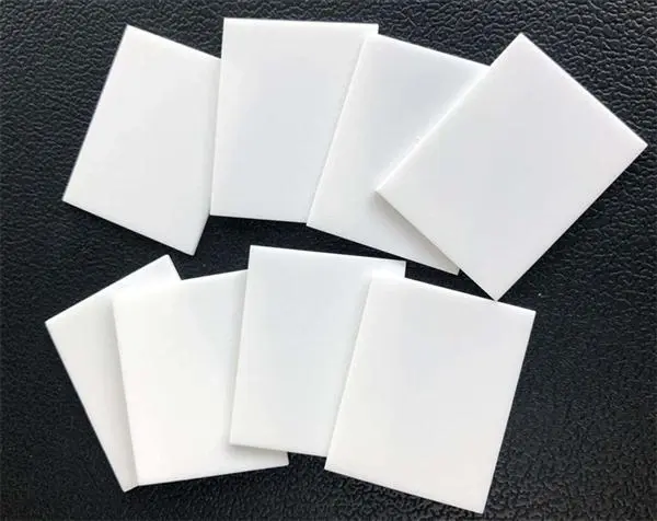
A ceramic substrate is a special type of board made by directly bonding copper foil to the surface of an oxide or a ceramic sheet at high temperature. The copper is joined to the ceramic by a high temperature process so the metal and the ceramic form a stable base for circuits.
a. They have high mechanical strength. They can hold parts and also act as support structures.
b. They are easy to machine. They keep accurate dimensions. They can be made into many layers.
c. Their surface is smooth. They do not warp, bend, or show small cracks.
a. They have high insulation resistance and high breakdown voltage. This keeps the circuits safe from shorting and from high voltage damage.
b. They have low dielectric constant and low dielectric loss. This helps signals pass with less loss.
c. Their performance stays stable at high temperature and high humidity. This helps ensure reliability in hard use conditions.
a. They have high thermal conductivity. This helps move heat away from hot parts.
b. Their thermal expansion coefficient can match related materials, especially silicon. This match reduces stress when parts heat and cool.
c. They have good heat resistance. They stay stable at high temperature.
a. They are chemically stable. They are easy to metallize. Circuit patterns stick well to them.
b. They do not absorb moisture. They resist oil and chemical attack. They release little radiation.
c. The materials used are harmless and not toxic. Their crystal structure does not change in the working temperature range.
d. Raw materials are abundant. The technology is mature. They are easy to make and the price is low.
Before firing the ceramic, there are four common forming methods. These are powder pressing (which can be mold pressing or isostatic pressing), extrusion, tape casting, and injection molding. Among these, tape casting is more often used in recent years for LSI packages and hybrid circuit substrates because it is easier to make many layers and it has higher production efficiency.
Common process routes are these three:
- Stack layers – hot press – remove binder – fire the base sheet – form circuit patterns – fire the circuit.
- Stack layers – print the circuit pattern on the surface – hot press – remove binder – co-fire.
- Print circuit pattern – stack – hot press – remove binder – co-fire.
In the thick film method, conductors (the circuit traces) and resistors are formed on the ceramic by screen printing. After printing, the parts are sintered to form the circuit and the contact pads. The binders used to fix the printed metal include glass type, oxide type, and mixed glass–oxide types.
Thin film uses vacuum methods like evaporation, ion plating, or sputtering to apply metal. Because thin film deposits metal from the gas phase, any metal can in principle be deposited. Also any substrate can in principle be metallized this way. But the thermal expansion of the metal film and the ceramic substrate should match as much as possible. It is also important to increase the adhesion of the metal layer to the ceramic.
Before firing, refractory metal pastes of Mo, W and similar metals are screen printed on the unfired ceramic sheets. The stack is then debindered and fired so the ceramic and the metal form one integral structure. This method has these features:
■ It can form very fine circuit lines and it is easy to make many layers, so high density wiring is possible.
■ Because the insulator and the conductor are formed together, hermetic sealing in packages is possible.
■ By choosing the right composition, forming pressure, and sintering temperature, the sintering shrinkage can be controlled. Especially when a substrate with zero in-plane shrinkage is made, this opens up use in BGA, CSP, and bare chip high-density packaging.
a. Raw material: Al₂O₃ is often made by the
Bayer process. In this method the raw material is bauxite, which includes hydrated aluminum oxides and related compounds.
b. Making: Al₂O₃ ceramics are usually formed by stacking unfired sheets. A binder like polyvinyl butyral (PVB) is often used. The firing temperature varies with added sintering aids, and is usually 1550–1600°C. Metalization methods for Al₂O₃ are mainly the thick film and co-firing methods. The pastes and the process technology are mature. They meet many application needs today.
c. Applications: Substrates for hybrid integrated circuits, LSI package substrates, and multilayer circuit substrates.
Mullite is one of the most stable crystalline phases in the Al₂O₃–SiO₂ system. Compared to Al₂O₃, mullite has a bit lower mechanical strength and lower thermal conductivity, but its dielectric constant is lower. This lower dielectric constant can help improve signal speed. Its thermal expansion coefficient is also low, which reduces thermal stress on mounted LSI. Also the expansion difference with conductor metals like Mo and W is smaller, so co-firing causes less stress between the metal and the ceramic.
a. Raw material: AlN is not a natural mineral. It is a man-made material first synthesized in the 1800s. Typical AlN powders are made by reduction nitridation or direct nitridation. The reduction nitridation method starts from Al₂O₃ and uses high-purity carbon to reduce it, then react with nitrogen to form AlN. The direct nitridation method reacts Al powder with N₂ to form AlN directly.
b. Making: The same forming methods used for Al₂O₃ substrates can be used for AlN. The most used route is stacking unfired sheets. For this, AlN powder, organic binders, solvent, and a surfactant are mixed to make a ceramic slurry. The slurry is tape cast, stacked, hot pressed, debindered, and then fired to make the AlN substrate.
c. AlN substrate features: AlN has thermal conductivity more than ten times that of Al₂O₃. Its coefficient of thermal expansion (CTE) matches silicon. Compared with Al₂O₃, AlN has higher insulation resistance and higher breakdown voltage. Its dielectric constant is lower. These features make AlN very valuable for package substrates.
d. Applications: Used for VHF band power amplifier modules, high power devices, and laser diode substrates.
a. Raw material: SiC is not a natural mineral. It is made by mixing silica, coke, and a little salt as powders. The mix is heated in a graphite furnace above 2000°C to react and form α-SiC. Then SiC can be purified by sublimation to get a dark green block of polycrystalline material.
b. Making: SiC has very high chemical and thermal stability, so normal firing methods make it hard to densify. Sintering aids and special firing methods are needed. Vacuum hot pressing is commonly used.
c. SiC features: A key feature is its very large thermal diffusion coefficient. It can even be larger than copper. Its thermal expansion is closer to silicon. But SiC has some downsides. Its dielectric constant is relatively high and its breakdown voltage is not as good as some other ceramics.
d. Applications: SiC substrates are used where high heat spreading is needed and voltage is not high. They are used for VLSI heat-sinking packages, high speed and high integration logic LSI with heat sinks, large computers, and laser diode substrates for optical communications.
BeO has thermal conductivity many times that of Al₂O₃. It works well for high power circuits. Its dielectric constant is low, so it is suitable for high frequency circuits. BeO substrates are usually made by dry pressing. They can also be made by the unfired sheet route with small additions of MgO or Al₂O₃. Because BeO powder is toxic, BeO products raise environmental and health concerns. In Japan BeO substrate production is not allowed and BeO must be imported from places like the United States.
From structure and making methods, ceramic substrates can be grouped into HTCC, LTCC, TFC, DBC, DPC, and so on. Ceramic substrates are used more and more in electronic packaging and in power electronics like IGBT (insulated gate bipolar transistor), LD (laser diode), high power LED, and CPV (concentrator photovoltaic) because of their good thermal conductivity, heat resistance, insulation, low thermal expansion, and falling cost.
Common ceramic base materials are BeO, Al₂O₃, AlN, and Si₃N₄. Among these, Si₃N₄ has very high electrical insulation and chemical stability. It also has good thermal stability and high mechanical strength. It can be used for high density and high integration circuit boards.
HTCC is high temperature co-fired ceramic substrate. To make HTCC, first ceramic powder such as Al₂O₃ or AlN is mixed with an organic binder. The mix is made into a paste and then formed into sheets by doctor blade or similar methods. The dried sheets become green bodies. Holes for vias are drilled and conductor pastes are screen printed for wiring and via filling. Then the green sheets are stacked and placed into a high temperature furnace around 1600°C for sintering. Because the sintering temperature is high, the choice of conductor metals is limited. Metals with high melting points but lower conductivity are used, such as tungsten, molybdenum, and manganese. The cost is high and thermal conductivity ranges roughly 20–200 W/(m·°C).
LTCC is low temperature co-fired ceramic. Its making steps are similar to HTCC. The difference is that the Al₂O₃ powder includes 30–50% by mass of low melting point glass. This lowers the firing temperature to about 850–900°C. Because the firing temperature is low, conductive metals with good conductivity like gold and silver can be used for electrodes and traces. LTCC uses screen printing for metal lines. This method can have alignment errors because of mesh stretch. Also when multilayers are stacked and co-fired, different shrinkage can occur and that hurts yield. To raise LTCC thermal conductivity, thermal vias or conductive vias can be added in the component areas, but that raises cost.
Compared to LTCC and HTCC, TFC is a post-fired ceramic substrate. It uses screen printing to apply metal pastes on the ceramic base surface. After drying, the part is fired at high temperature (700–800°C). Metal pastes are made of metal powder, organic resin, and glass. After firing, the resin burns off and the layer left is mostly metal bound by a glassy adhesive on the ceramic surface. The fired metal layer thickness is typically 10–20 μm and the minimum line width is about 0.3 mm. Because the technology is mature, the process is simple and cost is low, TFC is used where pattern precision needs are not high.
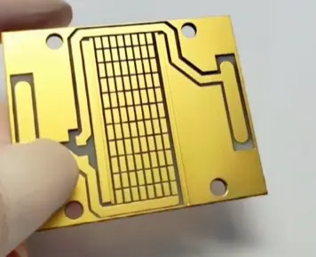
DBC is made by co-sintering or eutectic bonding copper foil to a ceramic sheet at high temperature (about 1065°C). After bonding, circuit patterns are formed by etching. Because copper foil has good electrical and thermal conduction and Al₂O₃ can control the expansion of the Cu–Al₂O₃–Cu composite, the DBC has a thermal expansion close to that of alumina. DBC has good thermal conduction, strong insulation, and high reliability. It is widely used in IGBT, laser diode, and CPV packaging. DBC has drawbacks. The high temperature eutectic reaction between Cu and Al₂O₃ needs strict control of equipment and process, so cost is higher. Micro-pores can form between Al₂O₃ and Cu, lowering thermal shock resistance. Copper foil can warp at high temperature, so the copper thickness on DBC is usually more than 100 μm. Also etching is used to form patterns, so minimum line width is generally more than 100 μm.

DPC starts with cleaning and pretreating the ceramic sheet. Then a Ti/Cu seed layer is deposited by vacuum sputtering on the substrate surface. Photolithography, development, and etching are used to form the circuit pattern. Then electroplating or chemical plating is used to grow the circuit thickness. After removing the photoresist the substrate is complete. DPC has these advantages: low temperature process (below 300°C), so it avoids the drawbacks of high temperature to materials and circuits and lowers manufacturing cost. Using thin film and photolithography makes the metal lines on the substrate finer. So DPC is well suited for packages that need high alignment accuracy. But DPC has downsides too. The electroplated copper thickness is limited, and electroplating waste liquid can cause pollution. The adhesion between metal layer and ceramic is lower, so the product reliability may be less.
When choosing a ceramic substrate, match the material to the application needs. If you need high thermal conductivity and a thermal expansion close to silicon, AlN or SiC may be best. If cost and mature processing matter, Al₂O₃ is a solid choice. If you need fine lines and low temperature processing, DPC and LTCC can work. If you need high density multilayer wiring and hermetic sealing, co-fired routes like LTCC or HTCC with co-sintered metal may be right.
Common application areas include power modules, RF power amplifiers, laser diode modules, high power LEDs, and high density LSI packaging. Power electronics gain from ceramic substrates because they move heat well and keep insulation and mechanical strength under thermal stress. RF devices gain from low dielectric loss and stable dielectric properties. High density packaging gains from the ability to make fine lines and to stack many layers with good alignment control if the process is suitable.
Every ceramic type and every process has tradeoffs. HTCC uses high firing temperature and so uses refractory metals for conductors. This limits conductivity and raises cost, but HTCC can be very robust at high temperature. LTCC lowers firing temperature by adding glass so better conductors can be used, but LTCC can have shrinkage issues and alignment trouble in multilayers. TFC is cheap and simple, but it cannot give very fine patterns. DBC gives excellent heat spread with thick copper, but its patterning limit and manufacturing cost can be issues. DPC allows fine patterning and low temperature processing, but adhesion and waste control need care.
Co-firing means printing metal pastes on the green ceramic and firing everything together. This can make very small features and true multilayer wiring. It also lets the ceramic and metal become one integrated body, which helps hermetic sealing. But co-firing needs careful control of materials to match shrinkage and sintering. Post-firing metallization, like thick film or thin film on fired ceramic, avoids co-sintering shrinkage issues. It can be easier for single layer or simple double layer needs. But post-fired methods may not reach the same wiring density and may have different adhesion or thermal properties.
- For co-fired multilayer substrate: make ceramic slurry, tape cast, drill vias in green tape, print conductor pastes by screen, stack tapes, press and debind, and then fire. After firing, do final processing like pad metallization and circuit etching if needed.
- For thick film on ceramic: use fired ceramic substrate, screen print conductor and resistor pastes, fire at 700–800°C, then trim resistors and add final metal pads.
- For DPC: clean ceramic, deposit Ti/Cu seed by sputter, pattern photoresist, etch seed to make pattern, electroplate to grow copper, strip resist, and final clean.
Ceramic PCB are a class of substrate materials that give unique strengths for electronic packaging. They offer good thermal paths, stable electrical behavior at temperature, and good mechanical strength. Different ceramic choices and different metallization routes let designers balance cost, thermal performance, electrical performance, and fine line pattern needs. Because of this, ceramic substrates are widely used in power electronics, RF modules, laser and diode packages, high power LEDs, and many high density packaging fields.