
Metal-Core PCB Capabilities
FLJ PCB supports aluminum and copper-based PCB constructions for designs with defined heat-transfer needs. Separate tables keep substrate and circuit capabilities clear.
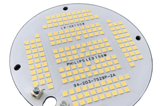
Metal substrates for a defined thermal path
A metal-core PCB combines conductors with an insulating structure and a metal base. The substrate helps transfer heat toward the cooling arrangement.
Aluminum and copper-based constructions serve LED, power and other thermally demanding electronics. The design still needs an appropriate dielectric, circuit copper, mounting interface and cooling path. A metal base alone does not establish operating temperature or heat dissipation of the finished product.
FLJ publishes separate aluminum and copper-based tables. These are more useful for construction review than combining the largest sizes or thinnest features into one universal specification. We connect the substrate to the mechanical and assembly requirements.
Aluminum PCB manufacturing capabilities
Published process ranges are matched to your material and construction during engineering review.
The conductivity value belongs to the selected material system. Identify the dielectric and supplier data when comparing substrates. It should not be read as a guaranteed whole-board or finished-product thermal result.
| Característica | Published aluminum capability |
|---|---|
| Finished copper | 18, 25, 35 or 70 μm |
| Grosor del tablero | 0.2–5.0 mm |
| Thickness tolerance at ≥1.0 mm | ±10% |
| Thickness tolerance below 1.0 mm | ±0,1 mm |
| Listed thermal conductivity | 1–12 W/m·K; material selection determines value |
| Minimum spacing | 0.2 mm |
| Hole tolerance | ±0,1 mm |
| Standard maximum size | 480 × 580 mm |
| Listed large size | 580 × 1180 mm |
| Outline accuracy | ±0,15 mm |
| Surface finishes | ENIG, immersion silver, immersion tin and OSP |
Copper-based PCB manufacturing capabilities
Copper-based structures provide a separate set of fabrication options.
Thermal-separation or pedestal constructions connect thermal design to a particular substrate structure. Share the component thermal pad and heat-transfer requirements so this route can be considered in the board review.
| Característica | Published copper-based capability |
|---|---|
| Capas | 1–8 |
| Product types | Single-sided, double-sided with core, single-sided multilayer and thermal-separation structures |
| Grosor del tablero | 0.5–5.0 mm |
| Finished copper scope | 1–3 oz in the stated process range |
| Maximum board size | 1200 × 480 mm |
| Minimum board size | 5 × 5 mm |
| Minimum drilling hole | 0.6 mm |
| Line / space at 1 oz | 4 / 5 mil |
| Line / space at 2 oz | 6 / 8 mil |
| Line / space at 3 oz | 10 / 11 mil |
| Outline tolerance | CNC ±0.15 mm; punching ±0.1 mm |
Dielectric, mounting and cooling details
Performance depends on the path from the component through the board to the cooling surface.
Dielectric thickness, electrical insulation, material conductivity and contact to the heat sink all matter. Holes and edge dimensions define product fit. Where isolation or working voltage matters, include those needs in the engineering conversation.
Finish and solder-mask choices also relate to assembly. LEDs, power packages and connectors can need different pad and stencil preparation. Material decisions should remain connected to soldering and inspection rather than becoming a separate purchase choice.
Insulation and thermal construction review
Send the thermal pad and cooling arrangement if available. We can help review the substrate choice and the material documentation.
| Construction item | What is reviewed | Data context |
|---|---|---|
| Dielectric layer | Thickness, thermal conductivity and insulation | Use the exact material grade data |
| Metal base | Alloy, thickness and cooling interface | Match stiffness, fit and heat transfer |
| Working voltage | Required isolation and dielectric performance | Review the intended circuit and material construction |
| Thermal path | Device pad, dielectric, metal and heat sink contact | Evaluate the complete product path rather than a single conductivity value |
Panel preparation and PCBA support
Outlines, spacing and handling need to suit fabrication and assembly.
Aluminum and copper substrates can involve different routing or punching arrangements. Panel layout, tooling and board support are discussed with the outline and component data. The goal is a practical route that preserves product fit and the board features that matter.
FLJ can coordinate components, assembly and testing with fabrication. Send available files, material preferences, quantity and thermal or mechanical information. If the substrate is not selected, describe the application and our engineers can help review the next decisions.
Frequently asked questions
Should I choose aluminum or copper?
The choice follows thermal path, construction, mechanical requirements and cost. Share the component and cooling arrangement so the comparison follows your product.
Does listed conductivity predict product temperature?
No. It describes material characteristics. Product temperature also depends on power, geometry, interfaces, cooling and operating conditions.
Can metal-core assembly be included?
Yes. We review the component mix and assembly route alongside the substrate and board specification.
Can I inquire without a substrate part number?
Yes. Send the board information and intended use. We can work through material options and missing details with you.
Explore related capabilities
Let’s review your next build
Send your available board files, drawings or project questions. Our team will review the information and follow up with you about the next step.