


人間にとって、熱すぎる身体は病気になる。電子機器にとって、部品は熱くなりすぎると故障する。信頼性が落ちる。だから、回路基板をよく冷やすことがとても重要なのだ。.
熱設計では、プリント基板が熱の主な担い手となります。プリント基板の熱は3つの場所から発生します:
- 電子部品からの熱。.
- プリント基板自体の熱。.
- システムの他の部分から来る熱。.
この3つのうち、部品からの熱が最も大きい。主な熱源である。次にプリント基板が発する熱。外部から来る熱は、システム全体の熱設計に依存する。.
実際のPCB設計では、エンジニアは多くの冷却項目について考えなければなりません。基板材料、部品選択、部品レイアウトなどです。以下では PCBレイアウト の段階だ。.
1.PCB冷却が重要な理由
PCB設計において冷却を最適化することは、デバイスの信頼性を維持し、長持ちさせるための鍵となります。レイアウト、配線、材料、構造を同時に考える必要があります。以下は、体系的な冷却戦略です。.
2.材料とスタックアップの最適化
高熱伝導性基材
- 熱伝導率の高いFR-4(例えば1.0W/m・K以上)を使用するか、メタルコアボードを使用する。.
- アルミ幅木の熱伝導率は約5~10W/m・K。.
- 高周波のシーンでは、セラミックボードを検討しよう。Al₂O₃は約24W/m・K。AlNは約180W/m・K。.
銅厚戦略
- 電源プレーンとグランドプレーンには、より厚い銅を使用する。例えば、2オンス(約70μm)以上の厚い銅を使用してください。.
- 大電流経路の場合は、3~6オンスの銅厚を追加してください。.
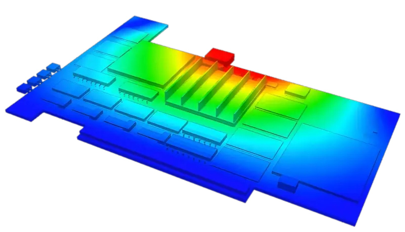
3.レイアウト冷却のヒント
部品レイアウト規定
- ホットパーツ(パワーMOSFET、ボルテージレギュレーター、ドライバーIC)は分散して配置する。一箇所に熱がこもらないように。.
- 敏感な部品(水晶振動子、ADC)は熱源から少なくとも5mm離してください。必要であれば、熱絶縁スロットを追加してください。.
- 基板の端やヒートシンクが取り付けられる場所の近くに高電力部品を置く。.
熱チャネル設計
サーマルパスの良い例:
[パワーIC] → [サーマルビアアレイ] → [インナー銅プレーン] → [ボードエッジサーマルパッド]
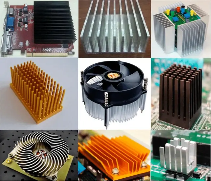
外部ヒートシンク
この経路は、ICからビア、内部銅、そして基板端または外部ヒートシンクへの熱を示す。.
4.銅の注入と銅の熱強化
銅注入の最適化
- パワーパーツの下にしっかりとした銅のエリアを作る。銅の面積は部品の面積の少なくとも3倍にしてください。.
- 可能な限りメッシュ状の銅を使う。メッシュは熱応力を下げます。多くのビアでメッシュをつなぐ。.
特殊銅構造
- スルーホールやキーパッドにサーマルリリーフパッドを使用して、はんだ接合部の低温化を回避してください。.
- 非常に高い電力領域には、銅インレイ技術を使う。これは基板に強固な銅ブロックを入れるものです。.
5.熱伝導ビアマトリックス
ビア・アレイ設計
- 熱源下でビアアレイを使用する。標準的なビアホールサイズ:0.3±0.05mm。このサイズは熱伝導と製造性のバランスをとっています。.
- ビアピッチ:ビア直径の1.5倍から2倍。アレイの規模は少なくとも5×5とする。.
- 充填スキーム:
- コスト優先:樹脂充填ビアを使用。.
- 最高の熱伝導のために:電気メッキされたフィルド・ビアを使用してください。これにより、熱伝導率を40%以上上げることができます。.
コネクション戦略
- 多層基板の場合は、すべての電源プレーンとグランドプレーンにビアを通す。.
- 片面基板の場合は、裏面に銅のアイランドとビアグループを追加し、熱を逃がしやすくする。.
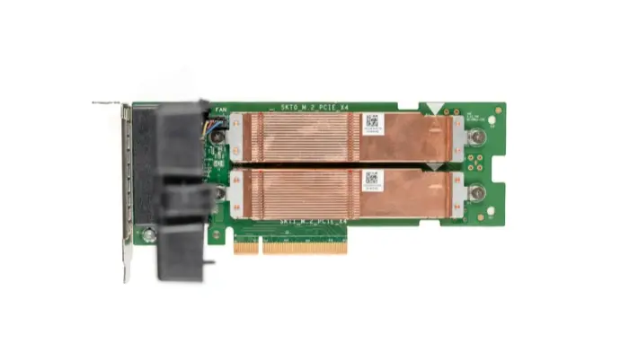
6.外部冷却とボードレベルの統合
ボードレベルの冷却統合
- ヒートシンク取り付け用の穴をあける。1mmのクリアランスでM3ネジを使用する。.
- ソルダーマスクのパワーパーツの下に窓を作る(はんだマスク 定義されたウィンドウ)を使って熱インターフェースを改善した。.
インターフェース素材の選択
| 素材タイプ | 熱伝導率 (W/m-K) | ユースケース |
|---|---|---|
| サーマルグリース | 1 - 5 | 小さな隙間を埋める (< 0.1 mm) |
| サーマルパッド | 3 - 12 | 中間の隙間 (0.2 - 1 mm) |
| 相変化材料 | 5 - 8 | 凹凸を自動で埋める |
| リキッドメタル | 15 - 80 | 非常に高い出力密度のケース |
ギャップの大きさとパワー密度に見合ったインターフェイス材料を選ぶ。.
7.強制空冷設計
エアフローに合わせたレイアウト
- ヒートパーツを空気の流れ方向に合わせます。これにより、下流の部品が過熱するのを防ぐことができます。.
- 高い部分の周囲には、少なくとも3mmの空気の通り道を確保する。.
- エアフローを誘導し、冷却経路を改善するために、ボードレベルのダクトを追加する。.
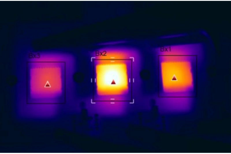
8.熱シミュレーションと検証
シミュレーションフロー
以下の手順を使用する:
- 3Dモデルを作る。.
- 熱境界条件を設定する。.
- 定常解析または過渡解析を実行します。.
- 温度フィールドを可視化する。.
- ホットスポットが85 °Cを超えていないか確認する。.
- もしそうなら、レイアウトと冷却を最適化する。.
- いいえ」の場合は、サーマルリスクレポートを出力する。.
一般的なツールANSYS Icepak、FloTHERM XT、Simcenter FLOEFD。.
9.工程上の注意と製造上の注意
はんだ付けの信頼性
- パッドの中央に直接サーマルビアを配置することは避けてください。代わりに交差したサーマルリリーフパターンを使用してください。.
- ウェーブはんだ付けの場合、はんだが流れ込むのを防ぐため、部品側のサーマルビアを埋めるかマスクする。.
熱応力制御
- リフローはんだ付け温度を満たすために、高Tg材料(Tg ≥ 170 °C)を使用してください。.
- 大きな銅のゾーンは、ボードの反りを避けるため、両側でバランスを取らなければならない。.
10.主な設計ルール
- 電力密度が0.05W/cm²を超える場合は、特別な熱設計が必要です。.
- 部品のジャンクション温度(T_j)を、データシートに記載されている制限値の80%以下に保ってください。.
- CPUやFPGAのような複雑なチップには、熱抵抗マトリックスモデルを使用します:
T_j = T_a + Σ(P_i × θ_ji)
ここで、T_jはジャンクション温度、T_aは周囲温度、P_iはソースiの電力、θ_jiはソースiからジャンクションjまでの熱抵抗である。.
11.プリント基板自体による冷却
一般的なPCB基材は、銅張りのエポキシ・ガラス生地やフェノール・ガラス生地である。紙ベースの銅張り基板を使う基板もいくつかある。これらの材料は電気的、加工的特性は良いのですが、熱伝導が良くありません。高温部品の場合、PCB樹脂の熱伝導に頼ることはできません。熱は部品表面から空気中に逃げなければなりません。.
今日、電子機器はよりコンパクトになっている。部品は近くに配置され、より多くの熱を発生する。部品の表面積が小さいと、部品を冷却するのに十分ではありません。また、QFPや BGA はPCBに熱を通します。ですから、最善の解決策は、PCB自身の熱を逃がす能力を向上させることです。PCBに熱を伝導または放出させるのです。.
部品パッケージの選択
- 熱設計を計画する際には、パッケージ・データとその熱伝導スペックを読んでください。.
- パッケージと基板間に良好な熱経路を設ける。.
- 熱経路上の空隙を避ける。隙間がある場合は熱伝導材で埋める。.
12.核となる考え方熱抵抗の最小化
熱設計とは、熱抵抗をできるだけ小さくすることです。これらの戦術を駆使してください:
- より低い伝導抵抗: より厚い銅、高熱の基材。.
- ヒートパスを短くする:ヒートシンクや内部銅プレーンに直行するビアを使う。.
- 表面積を増やす:銅の注ぎ口を広げ、フィンを追加する。.
- 熱交換の改善:強制空冷または液冷を使用する。.
実際の設計では、コスト、スペース、製造性のバランスを取る必要があります。多くのオプションを試し、それぞれについてシミュレーションを使用してください。プロトタイプでは、基板上にいくつかの冷却オプションを残しておきます。例えば、ヒートシンク取り付け用の穴、熱電対テストポイント、ファンコネクタなどです。これにより、チューニングが容易になります。.
13.最終ノート
優れた熱設計には、レイアウトのルールと基板の選択の両方が必要です。慎重な部品配置、広い銅、ビアアレイ、優れたインターフェイス材料を使用してください。熱シミュレーションと実際のプロトタイプでテストしてください。部品のジャンクション温度をデータシートの制限値以下に保つこと。サービスポイントとテストポイントを計画する。これにより、リスクを低減し、製品の安全性と信頼性を保つことができます。.

