
For people, a body that is too hot makes them sick. For electronics, parts fail when they get too hot. Their reliability drops. So, it is very important to cool circuit boards well.
In thermal design, the PCB is the main carrier of heat. The heat on a PCB comes from three places:
- Heat from electronic parts.
- Heat from the PCB itself.
- Heat that comes from other parts of the system.
Among these three, the heat from parts is the largest. It is the main heat source. Next is heat made by the PCB. Heat that comes from outside depends on the whole system thermal design.
In real PCB design, engineers must think about many cooling items. These include board material, part choice, and part layout. Below I focus on cooling in the PCB layout stage.
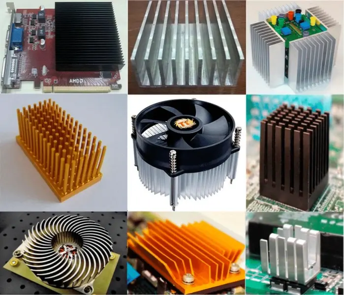
1. Why PCB Cooling Matters
Optimizing cooling in PCB design is key to keep devices reliable and to make them last. You must think about layout, routing, material, and structure at the same time. The following are systematic cooling strategies.
2. Materials and Stack-up Optimization
High thermal conductivity base materials
- Use high thermal FR-4 with higher thermal conductivity (for example ≥ 1.0 W/m·K) or use metal core boards.
- For an aluminum-core PCB, distinguish the conductivity of the aluminum base from that of the insulating dielectric. Compare the stack’s thermal resistance, including dielectric thickness and heatsink contact, rather than assigning one conductivity to the complete board.
- For high frequency scenes, consider ceramic boards. Al₂O₃ has about 24 W/m·K. AlN has about 180 W/m·K.
Copper thickness strategy
- Use thicker copper for power and ground planes. For example, use 2 oz (about 70 μm) or thicker.
- For high current paths, add local copper thickness of 3 to 6 oz. Use a stepped copper design.
3. Layout Cooling Tips
Part layout rules
- Place hot parts (power MOSFETs, voltage regulators, driver ICs) spread out. Do not let heat build up in one spot.
- Keep sensitive parts (crystals, ADCs) at least 5 mm away from heat sources. If needed, add thermal isolation slots.
- Put high power parts near board edges or near places where a heatsink can mount.
Thermal channel design
A good thermal path example:
[Power IC] → [Array of thermal vias] → [Inner copper plane] → [Board edge thermal pad]
          ↘ [External heatsink]
The path shows heat from the IC to vias, then to internal copper, then out to board edge or to an external heatsink.
4. Copper Pour and Copper Heat Enhancements
Copper pour optimization
- Create solid copper areas under power parts. Make the copper area at least three times the part area.
- For heat spreading, compare solid copper with any required patterned copper. A mesh reduces the available copper cross-section; use it only when mechanical or fabrication requirements justify the thermal tradeoff.
Special copper structures
- Use thermal relief pads in through-hole or key pads to avoid cold solder joints.
- For very high power regions, use copper inlay technology. This places a solid copper block in the board.
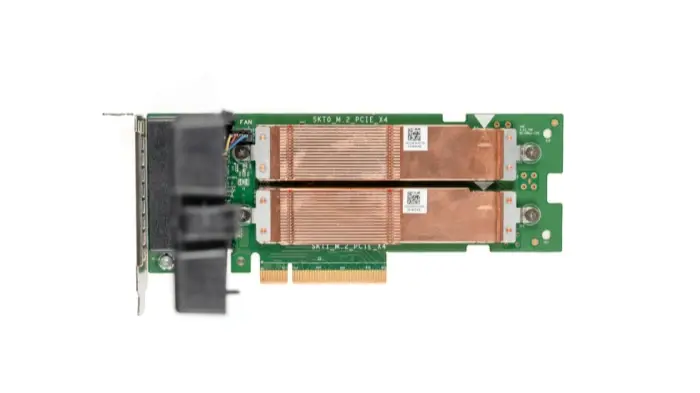
5. Via Matrix for Heat Transfer
Via array design
- Use via arrays under heat sources. Typical via hole size: 0.3 ± 0.05 mm. This size balances heat transfer and manufacturability.
- Choose via pitch and array size from pad diameter, annular ring, required copper clearance, package guidance and thermal analysis. Hole diameter alone does not define a manufacturable pitch.
- Filling scheme:
- Cost prior: use resin-filled vias.
- Copper-filled vias can improve a thermal path, but the result depends on geometry and the rest of the stack; confirm the fill process and thermal model with the fabricator.
Via connection strategy
- For multilayer boards, connect thermal vias only to copper on the intended electrical net. Provide antipads at other power and ground planes to prevent shorts.
- A single-sided copper board has no backside copper plane to connect through. If backside copper and plated vias are needed, review a two-sided or another suitable construction with the fabricator.
6. External Cooling and Board-level Integration
Board-level cooling integration
- Leave holes for heatsink mounting. Use M3 screws with 1 mm clearance.
- Make windows under power parts in the solder mask (solder mask defined window) to improve the thermal interface.
Interface material selection
| Material Type | Thermal Conductivity (W/m·K) | Use Case |
|---|---|---|
| Thermal grease | 1 – 5 | Fill small gaps (< 0.1 mm) |
| Thermal pads | 3 – 12 | Medium gaps (0.2 – 1 mm) |
| Phase change material | 5 – 8 | Auto fill uneven surfaces |
| Liquid metal | 15 – 80 | Very high power density cases |
Pick the interface material to match gap size and power density.
7. Forced Air Cooling Design
Layout to match airflow
- Align heat parts in the air flow direction. This keeps downstream parts from overheating.
- Leave at least 3 mm of clear air path around high parts.
- Add board-level ducts to guide air flow and to improve cooling paths.
8. Thermal Simulation and Verification
Simulation flow
Use the following steps:
- Build a 3D model.
- Set thermal boundary conditions.
- Run steady state or transient analysis.
- Visualize the temperature field.
- Compare measured or simulated temperatures with the applicable component, laminate, connector and interface limits at the specified worst-case ambient.
- If yes, optimize the layout and cooling.
- If no, output the thermal risk report.
Common tools: ANSYS Icepak, FloTHERM XT, Simcenter FLOEFD.
9. Process Notes and Manufacturing Care
Soldering reliability
- Thermal vias in an exposed thermal pad may be required by the package design. Specify via filling or capping and paste apertures with the assembler to control solder loss; thermal-relief spokes can impede the intended heat path.
- For wave soldering, fill or mask thermal vias on the component side to avoid solder flowing through.
Thermal stress control
- Use high Tg materials (Tg ≥ 170 °C) to meet reflow soldering temperatures.
- Large copper zones must be balanced on both sides to avoid board warping.
10. Key Design Rules
- If power density > 0.05 W/cm², you must do special thermal design.
- Set a junction-temperature margin below the datasheet limit using the product’s reliability requirements and worst-case operating conditions; a percentage of a Celsius rating is not a general derating rule.
- For complex chips like CPUs and FPGAs, use a thermal resistance matrix model:
T_j = T_a + Σ(P_i × θ_ji)
Where T_j is junction temperature, T_a is ambient, P_i is power of source i, and θ_ji is thermal resistance from source i to junction j. Use a validated system thermal model for θ_ji. A datasheet θ_JA measured on a specified test board does not by itself describe mutual heating between components.
11. Cooling via the PCB Itself
Common PCB base materials are copper-clad epoxy glass fabric or phenolic glass fabric. There are a few boards that use paper-based copper-clad boards. These materials have good electrical and processing properties, but they do not conduct heat well. For hot parts, you cannot rely on the PCB resin to carry heat away. Heat must go from the part surface to the air.
Today, electronics are more compact. Parts sit close together and produce more heat. Small part surface area is not enough to cool parts. Also, many surface mount parts like QFP and BGA pass heat into the PCB. So, the best solution is to improve the PCB’s own ability to carry heat away. Let the PCB conduct or emit the heat.
Part package selection
- When you plan thermal design, read the package data and its thermal conduction specs.
- Provide a good thermal path between the package and the board.
- Avoid air gaps on the thermal path. If gaps exist, fill them with thermal materials.
12. The Core Idea: Minimize Thermal Resistance
Thermal design is about making the thermal resistance as small as possible. Use these tactics:
- Lower conduction resistance: thicker copper, high thermal base materials.
- Shorten heat paths: use vias that go straight to heatsinks or internal copper planes.
- Increase surface area: expand copper pours and add fins.
- Improve heat exchange: use forced air or liquid cooling.
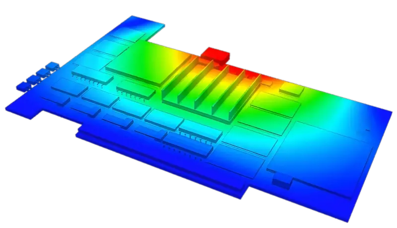
In real designs, you must balance cost, space, and manufacturability. Try many options and use simulation for each. On prototypes, leave several cooling options on the board. Examples: holes for heatsink mounting, thermocouple test points, and a fan connector. This makes tuning easier.
13. Final Notes
Good thermal design uses both layout rules and board choices. Use careful part placement, wide copper, via arrays, and good interface materials. Test with thermal simulation and with real prototypes. Keep part junction temperatures well under datasheet limits. Plan for service and test points. This lowers risk and keeps the product safe and reliable.