


PCBゴールドフィンガーとは?
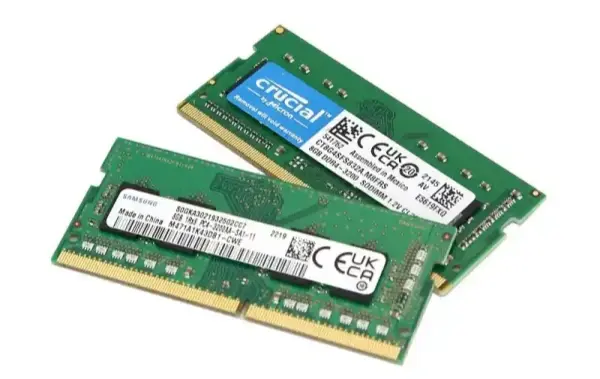
コンピューターのメモリースティックやグラフィックカードには、金色の導電性接点が並んでいる。人々はこれを “ゴールド・フィンガー ”と呼ぶ。PCBの設計と製造の分野では、ゴールド・フィンガー(「ゴールド・フィンガー」または「エッジ・コネクター」とも呼ばれる)は、基板をソケットに差し込むためのコネクターを使用する。ゴールド・フィンガーによって、基板はシステムの他の部分に接続される。.
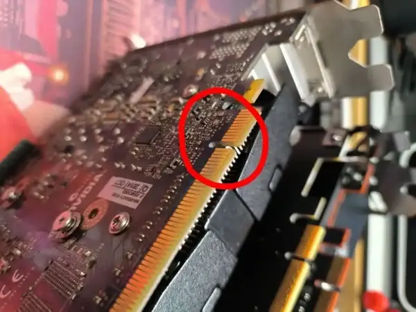
ゴールド・フィンガーは、PCBの一端をコネクター・スロットに挿入することで機能する。コネクタのピンは、ボードのパッドまたは銅のトレースに特定の場所で接触する。これにより、信号と電力が基板を出入りする経路が作られる。耐摩耗性と良好な接触のために、基板上のパッドや銅はニッケルや金でメッキされている。メッキされたパッドが指のように見えることから、人々はゴールド・フィンガーと呼ぶ。.
ゴールドフィンガーの種類
シェイプ別
一般的な形は2つある。ひとつは直線。もう1つは曲線です。まっすぐなゴールドフィンガーは、DDR、DDR2、DDR3、DDR3Lなどのメモリタイプに適合します。湾曲したゴールドフィンガーは、DDR4およびDDR5メモリースティックに適合します。.
ポジション別
ゴールド・フィンガーはPCBの片面または両面に付けることができる。片面ゴールド・フィンガーは基板の片側エッジにのみある。両面のゴールド・フィンガーは両端にある。両面タイプは、PCI、ISA、AGPのようなダブルスロットコネクタを使用するデバイスで一般的です。.
長さ別
ゴールドのフィンガーは、一列の長さがまちまちであることがある。あるコンタクトは長く、あるコンタクトは短い。設計者は、特定のピンに異なる機能や優先順位を与えるために、このようなことを行います。例えば、長いパッドは電源ピン、グランドピン、リセットピンを示します。.
ゴールドフィンガーPCBにはどのような表面処理が施されていますか?
ゴールドフィンガーには、主にいくつかの表面処理が施されている。.
電気めっきニッケル-金(ハードゴールド)
その厚さは3~50マイクロインチに達する。導電性に優れ、酸化に強く、摩耗しにくいため、頻繁に抜き差ししたり、機械的な摩擦にさらされたりするゴールド・フィンガーにはハード・ゴールドが使われる。硬質金は高価です。そのため、基板全体ではなく、ゴールド・フィンガーのような小さな部分にのみ使用される。.
イマージョン・ゴールドエニグ)
一般的な厚さは1マイクロインチ程度で、3マイクロインチまで可能である。無電解金は導電性、平坦性、はんだ付け性に優れている。設計者は、キーやボンディングIC、BGA部品を搭載した高精度基板に使用する。金指にそれほど高い耐摩耗性が必要ない場合は、基板全体に無電解金を使用することができます。無電解金は電気メッキの硬質金よりもはるかに低コストです。無電解金は黄色く見えます。.
PCB金メッキプロセスとは?
PCBゴールドフィンガーの硬質金メッキの流れはこうだ:
-
ブルーインクの表紙(カバーマスク)
ハードゴールドが必要なゴールドフィンガーパッドを除き、PCB表面全体をブルーの保護マスクで覆う。導電部分が基板の方向と一致していることを確認する。.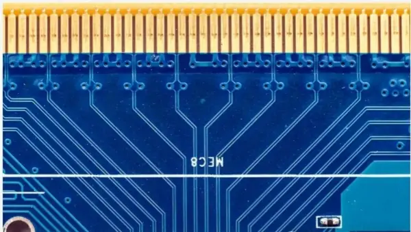
-
銅パッド表面の酸化物を取り除く
硫酸を使ってPCBの銅パッド表面の酸化膜を除去する。その後、銅の表面を水で洗い流します。その後、パッド表面をさらにきれいにするため、研磨またはスクラブを行います。次に、銅の表面を水と脱イオン水ですすぎます。. -
PCBパッド銅表面にニッケルをめっきする。
洗浄後、電流を流してニッケル層を金の指パッドの表面にめっきする。その後、水と脱イオン水でニッケルめっきパッドをすすぎます。. -
ニッケルめっきのPCBパッドに金をめっきする。
ニッケルめっきの後、電流を流してニッケルの上に金の層をめっきする。未使用の金は回収する。その後、金の指の表面をまず水で、次に脱イオン水ですすぎます。. -
青インクを取り除く
これでPCBゴールドフィンガー上のハードゴールドは完成です。青インクを取り除き、PCB加工を続けてソルダーマスク印刷ステップに進みます。.
上記のステップから、ゴールドフィンガー工程は複雑ではありません。それでも、ゴールドフィンガー工程を社内で行えるプリント基板工場は限られています。.
PCBゴールドフィンガーの使い方
1.エッジコネクター
ドーターPCBをメインマザーボードに接続する場合、PCI、ISA、AGPスロットなど、いくつかのメススロットのいずれかに差し込みます。これらのスロットを介して、ゴールドフィンガーが周辺機器やドーターカードとコンピュータ本体との間で信号を伝達します。.
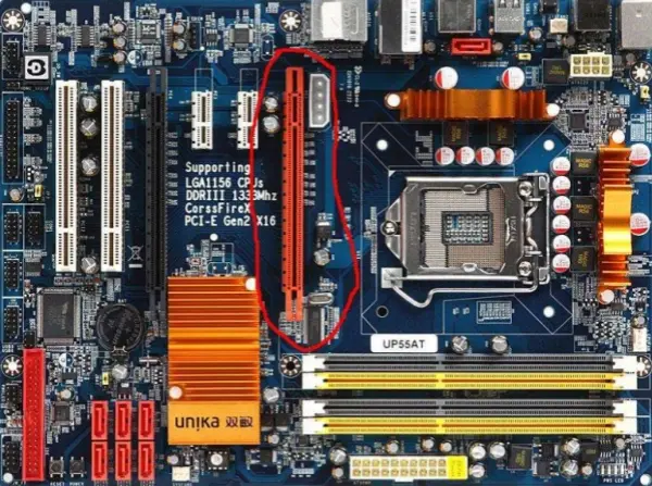
PCB上のPCIポートソケットは、多くの場合、片側が開くプラスチック製のハウジングである。長い方の端の片方または両方にピンがある。コネクタには、正しいカード・タイプがソケットに入るようにキーイング・バンプやノッチが含まれている場合がある。ソケットの幅は基板の厚みに応じて選択される。ソケットの反対側には、通常、リボンケーブル用の圧接コネクタがある。マザーボードやドーターカードも反対側で接続できる。.
2.特殊アダプター
ゴールド・フィンガーによって、パーソナル・コンピューターは多くの新しい機能を得ることができる。ドーターPCBをマザーボードに垂直に挿入することで、コンピューターはより優れたグラフィックスやハイファイ・サウンドを追加することができる。これらのカードは頻繁に抜き差しされるものではない。そのため、これらのカードのゴールド・フィンガーは通常、カードそのものよりも耐久性がある。.
3.外部接続
コンピュータステーションに追加された周辺機器は、PCBゴールドフィンガーを介してマザーボードにリンクすることができる。スピーカー、サブウーファー、スキャナー、プリンター、モニターなどのデバイスは、コンピュータタワーの背面にあるスロットに差し込みます。これらのスロットはPCBに接続され、PCBはマザーボードに接続される。.
PCBゴールドフィンガー設計ルール
-
メッキのスルーホールは、ゴールドの指から離すこと。. ビアやメッキの穴は、エッジの接触部分に近づけないこと。.
-
頻繁に抜き差しが必要なボードにはハードゴールドを使用する。. 硬質金は耐摩耗性を高める。化学ニッケル/無電解金は硬質金より安い。しかし、無電解金は耐摩耗性が劣る。.
-
ゴールドの指には面取りが必要だ。. 一般的な角度は45度。20度や30度といった角度も使われる。面取りを省略した設計の場合、挿入時に問題が生じる可能性がある。.
-
金指の部分全体にソルダーレジストを開ける。. ピンにソルダーマスクステンシルを使用しないでください。.
-
はんだまたは銀パッドから指先までの最短距離は14ミル。. パッドは、ビアパッドを含め、ゴールドフィンガー部分から少なくとも1mm離すことを推奨する。.
-
金指の表面に銅が露出したままにしないこと。. 接触面にはメッキを施す。.
-
インナーレイヤーのゴールドフィンガーの下の銅をカットする。. ゴールド・フィンガー以下のすべての内層は銅を除去する必要がある。通常、銅のキープアウト幅は3mmである。ハーフフィンガーでもフルフィンガーでも銅をカットできます。PCIe 設計では、ゴールド・フィンガー下の銅は完全に除去されるべきという証拠もあります。.
ゴールド・フィンガーは一般的な信号トレースよりもインピーダンスが低い。フィンガーの下の銅をカットすることで、ゴールド・フィンガーと隣接するインピーダンス制御ラインとの間のインピーダンス差が小さくなる。これはESD対策にも役立ちます。.
無電解ゴールドとゴールド・フィンガーの違い
簡単に言えば、ゴールド・フィンガーとは真鍮や銅の接点部分のことである。無電解ゴールドは、PCBに使用される表面仕上げの一種です。.
金は酸化に強い。また、金は電気をよく通す。メモリースティックでは、メモリースロットと嵌合する部品が金でメッキされ、信号が金のフィンガーを通過するようになっている。ゴールド・フィンガーとは、黄色い導電性コンタクトのこと。これらの接点は表面に金メッキが施され、指のように配置されている。そのため、指のように見えることからこの名前がついた。.
わかりやすく言えば、ゴールドフィンガーとはメモリースティックのメモリースロットとの接続部分のことである。すべての信号は金指を通過する。.
ゴールド・フィンガーは銅クラッド基板から作られる。その後、コンタクト部分は特殊な工程で金の層でメッキされる。.
つまり、簡単に言えば、無電解金(ENIG)は基板に施される表面仕上げの一種である。ゴールドフィンガーとは、基板とソケットの間で信号や導通を行う基板部分のことです。.
市場では、ゴールドの指の表面に本物のゴールドが使われているとは限らない。金は高価なのだ。現在、多くのメモリースティックは金の代わりに錫メッキを使っている。1990年代以降、錫が一般的になりました。現在では、ほとんどのマザーボード、メモリースティック、グラフィックカードが “ゴールドフィンガー ”に錫を使用している。今でも接点に金を使用しているのは、一部の高性能サーバーやワークステーションの部品だけです。そのような部品ははるかに高価です。.
概要
ゴールド・フィンガーは、ソケットに差し込むプリント基板の端の接点である。基板を他の部品に接続するためのもの。基板のパッドをニッケルと金でメッキして作られる。ゴールド・フィンガーには、様々な用途に応じた形状、位置、長さがあります。表面仕上げには、硬質金メッキと無電解金メッキがある。摩耗には硬質金が最適です。無電解金メッキは安価で、はんだ付けが可能です。設計者は、パッドやビアをコンタクトエッジから離さなければならない。面取りをし、ソルダーレジストを開けなければならない。指の下の銅は通常切り取る必要がある。市場慣行は、コストの問題から、多くのコンシューマー製品で本物の金メッキから錫メッキに移行した。特殊な機器やサーバー・レベルの機器に限っては、今でも本金を使用していることが多い。.