
Selective hard gold · Finished mating edges
Gold Finger PCB Manufacturing
Hard-gold contacts, accurately formed board edges and a solderable finish for the rest of your circuit.
FLJ manufactures gold finger PCBs for plug-in modules, expansion cards and board-to-board connections. From prototypes to production, we combine selective nickel and hard-gold plating with profiling and beveling to produce the contact edge specified for your connector.
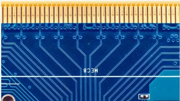
A contact pattern built for its socket
Gold Finger PCB Types and Specifications
Gold fingers are conductive lands at the edge of a PCB that engage spring contacts inside a mating connector. Their position, reach and finished board thickness work together to establish that interface.
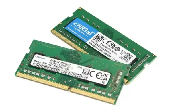
Uniform, Staggered and Segmented Contacts
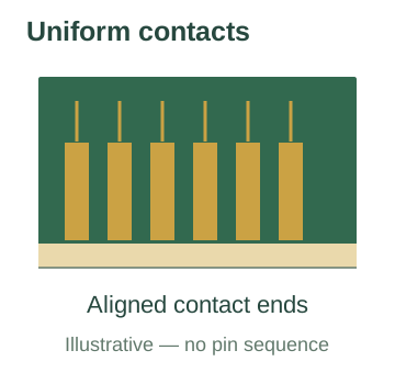
Uniform contacts
Equal-length fingers reach the same position along the insertion direction. This layout suits connector designs with a common contact length and alignment.
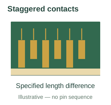
Staggered contacts
Selected fingers extend farther than others. The length difference supports staged engagement when required by the connector and circuit design.
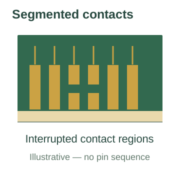
Segmented contacts
A specified contact pattern contains separate sections along its length. The segment positions and insulating interruptions follow the mating connector geometry.
Illustrative contact layouts. One- or two-face contacts and contacts on opposite board edges are separate construction choices.
Mating-Edge Specifications
FLJ supplies selective hard-gold contacts with ENIG or OSP on the soldering areas. The following fields define the contact edge and the manufacturing drawing.
| Feature | Manufacturing scope / specification |
|---|---|
| Contact layout | Uniform, staggered or segmented; contacts on one or both board faces as specified. |
| Selective finish | Nickel underlayer and electroplated hard gold in the contact region; ENIG or OSP on other exposed copper where specified. |
| Gold and nickel thickness | Separate gold and nickel callouts in µm or µin, with the contact region and measurement locations identified. |
| Finished board and tip thickness | Match the connector thickness window and the remaining thickness at the beveled tip. |
| Bevel angles | 20°, 30°, 45°; define the angle reference and required beveled section on the connector drawing. |
| Bevel angle tolerance | ±5° bevel-angle process reference, considered with the finished edge dimensions. |
- Lateral contact clearance 8 mil / 0.203 mm
- Finger side to finished profile edge. This locates the contact beside the board outline; entry-end and bevel dimensions are defined separately.
- Panel support tab 6 mm minimum
- Uninterrupted tab beside the fingers, used as the handling and breakaway reference in the panel design.
Use these mechanical references with the connector drawing. The finished thickness, contact reach and bevel section are specified together; see beveling and panel tolerances.
Two surface roles on one circuit
Hard Gold Contacts and Solderable Board Finishes
Copper, Nickel and the Gold Contact Surface
The copper land carries the circuit to the connector. A nickel underlayer separates the copper from the gold and supports the plated contact surface. Electroplated hard gold provides the exposed mating surface where the connector wipes along the finger during insertion and removal.
Specify gold and nickel thickness separately, including the unit. For a unit-conversion example, 30 µin = 0.762 µm. The selected coating thickness follows the contact duty and drawing, while finished board thickness controls the mechanical fit in the socket.
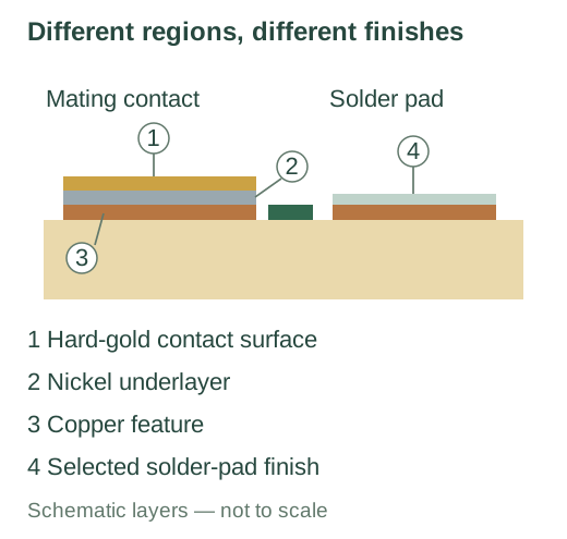
Selective Hard Gold with ENIG or OSP
The connector and component pads have different jobs. Hard gold is selected for the sliding contact, while the component pads need a finish suited to soldering. Selective processing allows both functions on the same PCB.
FLJ combines ENIG with gold fingers or OSP with electroplated gold. The drawing identifies the contact boundary and the finish on the remaining exposed copper so that pads intended for assembly receive the specified solderable treatment.
From exposed copper to a plated mating edge
Selective Plating and Edge Finishing
Gold finger manufacture joins two operations: building the contact surface and shaping the board that carries it. The production panel provides the handling support and electrical connections needed before the final outline is released.
Preparing the Contact Area and Plating Connections
The contact copper is cleaned and prepared for plating. Protection over adjacent areas confines treatment to the specified region, keeping the contact process separate from the finish required on component pads.
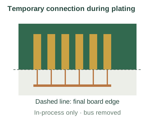
Electroplating needs a conductive path to each finger. Temporary production connections supply that path while the board remains in its panel. In the uniform-finger example, feeds extend to a common bus beyond the future outline; profiling removes the temporary conductive links.
Long-and-short fingers need particular attention: a shortened contact may not reach that common bar. Its current path and removal method must preserve the specified contact length and final electrical isolation. Segmented patterns likewise need the production connection plan to follow the actual contact sections.
Building the Nickel and Hard Gold Layers
Nickel is deposited over the prepared contact copper, followed by electroplated hard gold. Plating distribution depends on the contact pattern and production electrical connections as well as the specified layer thickness.
Processing coordinates the selectively plated contacts with ENIG or OSP elsewhere on the board. Protection is removed as required by the route, and the completed panel proceeds through the remaining finish, outline and edge operations.
Checking the Finished Contact Surface
Inspection covers the plated contact area, coating thickness and adhesion, together with scratches, exposed underlying material or unwanted deposits. Measurement locations are associated with the contact pattern so that a thickness record describes the specified region.
The final checks also examine the contact outline, bevel and cleanliness. PCB electrical testing verifies continuity and isolation; coating condition and connector wear require their own checks.
The coating meets the mechanical interface
Bevel Geometry and Connector Fit
A bevel forms the lead-in at the mating edge. Its angle, axial run and remaining tip thickness determine the section entering the connector, while the full finished thickness must fit the socket’s board-thickness range.
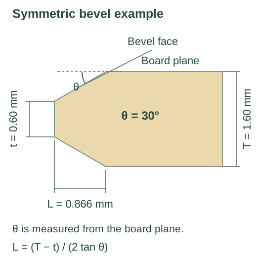
Board Thickness, Remaining Tip and Angle
Define the angle from an explicit reference. For a symmetric two-sided bevel, θ is measured from the board plane, T is finished board thickness and t is the remaining tip thickness. The axial run L is measured along the board plane:
For example, T = 1.60 mm, t = 0.60 mm and θ = 30° give L ≈ 0.866 mm. Changing the angle while keeping both thicknesses fixed changes the run. These dimensions should therefore be read together rather than selecting an angle alone.
Contact Ends, Copper Clearance and Panel Support
Locate the contact ends and nearby inner-layer copper against the actual material removed by beveling. Lateral side clearance is measured beside the contact at the finished outline; the insertion-end geometry determines the contact reach and the copper kept clear of the cut. Together they preserve the usable contact region and keep internal copper within the laminate.
The uninterrupted support tab beside the fingers belongs to panel handling and breakaway planning. Its position and removal must leave the connector seating region usable. Our PCB fabrication review connects the copper, finished outline and panel support before tooling.
Need a particular contact reach, coating thickness or beveled section? Send FLJ the connector requirements for a manufacturing quote.