
Lead-Free PCB Assembly Services
SMT, through-hole and mixed-technology assembly with the solder system matched to your board and components.
FLJ connects component supply, soldering, selected rework and inspection in one assembly scope. From a new build to a tin-lead conversion, the materials and measured thermal response guide the work.

Lead-Free PCB Assembly Capabilities
FLJ assembles lead-free SMT, through-hole, and mixed-technology boards in single- or double-sided layouts. We coordinate the board finish, component terminations and solder materials with the operations needed to deliver your assembled board. Complete-product RoHS documentation covers more than the solder used in assembly.
- SMT and mixed-technology builds
- SMT assembly covers solder-paste printing, component placement, and reflow. Through-hole parts and local soldering can be added where the build calls for them, with specified inspection, programming, or testing included as agreed. See the SMT assembly process for broader process details.
- Board and component supply
- FLJ can coordinate bare boards and components with assembly, including customer-consigned parts. If a BOM line is unavailable, FLJ can propose and quote a substitute for customer approval; an approved change is then carried into the current build. The component sourcing process explains how approved alternatives are handled.
- Existing assemblies and selected rework
- Selected component removal, replacement and local soldering can extend an existing assembly. We match the repair material to the original joints, protect nearby parts during heating, and recheck the affected work. A tin-lead conversion also accounts for the board finish and component terminations.
Solder Alloys, PCB Finishes and Component Compatibility
For an FLJ assembly order, identify the required solder alloy and the materials already present on the board and components. Alloy name alone does not define the flux, deposit or soldering behavior: solder paste combines metal powder with flux for a controlled print or dispense, solder bar feeds a molten solder bath, and wire supplies solder locally for hand work. Match the form and its specific product requirements to the assembly process.
Lead-Free Solder Alloy Options
These representative nominal systems show why material identity matters. The compositions are mass percentages; they are examples for comparison, not a statement of FLJ stock. For SAC305, solidus marks the start of melting and liquidus the point at which the alloy is fully liquid. A eutectic alloy is listed at its single melting point.

| Alloy system | Nominal composition and melting | Typical process use | Selection considerations |
|---|---|---|---|
| SAC305 | Sn96.5Ag3Cu0.5; solidus 217°C, liquidus 220°C. | Commonly specified as paste for reflow; alloy is also available in other supply forms. | Choose the specific paste or other product: powder, flux, deposition and process requirements vary even under the SAC305 name. |
| Sn99.3Cu0.7 (Sn-0.7Cu) | Sn99.3Cu0.7; melting temperature approximately 227°C. | Solder bar for wave soldering is a typical application. | Confirm the selected grade and flux. Modified SnCu grades and the actual solder bath composition may differ. |
| Sn42Bi58 | Sn42Bi58; 138°C eutectic melting point. | A representative low-temperature lead-free option for a process requiring lower alloy melting temperature. | Check the exact alloy/product, existing joint metals and later thermal steps. The lower melting point alone does not establish suitability or joint performance. |
Matching Board Finishes and Component Ratings
Match the specified PCB finish to the soldering task and land geometry. ENIG soldering surfaces can provide flat lands for assembly; repeated-contact or wire-bond interfaces have different requirements. Identify the finish from the board specification rather than appearance. With leaded or lead-free HASL, the specified solder coating becomes part of the joint during later soldering. An existing SnPb coating therefore remains a source of lead even when lead-free paste is added.
Component compatibility depends on the actual termination or solder ball, package surface and its permitted peak temperature, alongside the selected solder product. Some BGA packages with SAC solder balls may not suit a lower-temperature traditional SnPb reflow profile. Moisture-sensitive device preparation also depends on the package label, opening history and storage condition; quantity or date code alone cannot establish readiness. For the order, provide the finish, part and package details, available handling history, and applicable component requirements so the materials and assembly route can be matched to the build.
Process Control for Lead-Free Soldering
Reflow Profiling for the Populated Board
Lead-free reflow is set around the selected solder alloy and paste, the assembled board, and the limits of its components. An alloy’s melting range describes when solder can become liquid; it does not specify the temperature every joint reaches or a complete oven recipe. Zone settings control the oven environment, while thermocouples attached at representative joints record the board’s local response.
We profile a populated, thermally representative build at joints with different heat demands, including heavy copper connections and large thermal-mass parts, as well as smaller or heat-sensitive locations. Copper planes and large packages absorb and spread heat, so a cooler measurement location may still be short of the wetting window while another location is already approaching a component limit. Measurements across the board expose that spread and guide adjustments to oven zones and conveyor speed.
Each part of the profile has a job: preheat limits temperature differences and lets flux volatiles escape; any soak gives the flux time to act on surface oxides; time above the alloy’s liquidus supports wetting and the solder-to-pad interface reaction; controlled cooling lets the joint solidify. We compare the measured joint profile with the selected solder product’s processing requirements. Separately, package-surface measurements are checked against the component’s permitted peak temperature and exposure duration. A package classification limit is not a joint-temperature target. Moisture-sensitivity requirements also govern the device’s handling and preparation. The usable process must satisfy these constraints together, including prior heat exposure.
Through-Hole and Local Soldering
Through-hole joints need heat to reach both the plated barrel and lead so solder can wet their surfaces and flow into the hole. Flux condition, preheat, contact, and the joint’s copper path all matter. Thick copper and connected planes draw heat away; increasing pot or tool temperature alone can overheat the lead, pad, or nearby laminate without correcting poor contact or inadequate preheat. Wave and selective soldering therefore depend on matching flux, board preheat, and solder contact to the actual assembly.
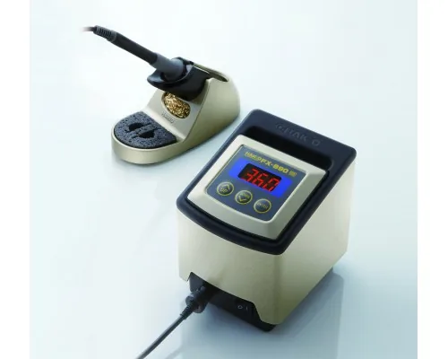
For hand soldering or local wire feed, the tip must transfer enough heat through a suitable contact area and remain accessible to the joint. On mixed or double-sided boards, previously installed parts, solder joints, supports, and nearby heat-sensitive components remain part of the thermal load during the next operation. The same applies to rework: protect adjacent parts and the board while delivering enough local heat for the target joint to wet. See our through-hole assembly process for the broader THT workflow.
Material Separation, Conversion and Rework
Identifying Solder Materials and Production Tools
A lead-free build depends on the metals already present on the board and components as well as the solder added during assembly. We identify the specified board finish and component terminations alongside the BOM, then match solder paste, wave or selective-solder bar, and hand-solder wire to that build route. A “lead-free” label on one reel or a bright-looking finish cannot establish the material state of every joint.
Solder remaining on a tip, in a solder pot or on other solder-contact tooling can enter the next joint. FLJ keeps solder materials and contact tools identified with the intended route. When work changes between tin-lead and lead-free materials, separation, cleaning or replacement addresses the relevant contact path; the choice depends on the tool and retained material. We retain the material identity for touch-up and repair, where a stray tin-lead deposit can change joint composition. Board finish and component termination details matter too: either can contribute metal when the joint is heated.
Transitioning or Reworking an Existing Assembly
Changing the stencil paste does not convert an assembled board. Existing SnPb joints, a tin-lead board finish, or component terminations remain in the connection and can mix with the replacement alloy. This matters at packages such as BGAs, where the original solder ball and new assembly solder form a combined joint; the original solder ball must be considered when selecting the reflow conditions and assessing the resulting joint. Bismuth-bearing low-temperature solder also needs particular evaluation where lead may remain, so a low melting point alone does not make it a general-purpose repair choice.
For component removal, the target connections must reflow before the part is lifted. Pulling against a partly solid joint can tear a pad from the laminate. After removal, we clear old solder as appropriate, inspect the lands, restore a suitable solder deposit and place the replacement before rebuilding the joint. Repair adds another heating event to the assembly’s history. Earlier interface reactions and any heat damage to the board or neighboring components remain relevant when choosing the next operation. We use the available build and component information to select compatible replacement materials; where a change in part is needed, approved component alternatives can be tied to the assembly route.
Lead-Free Joint Inspection and Build Records
Wetting, Joint Appearance and Hidden Connections
Lead-free solder can leave a joint with a different surface appearance from traditional tin-lead solder. A dull finish alone does not establish a cold joint or reveal lead content. Inspect wetting at the pad and lead, solder coverage and shape, and conditions such as poor wetting or bridging against the applicable workmanship criteria.
Automated optical inspection (AOI) assesses visible placement and solder features; X-ray supports examination of selected connections hidden beneath packages. Electrical and functional tests assess continuity or specified board behavior. Methods are selected for the package, board and agreed criteria; none alone establishes every aspect of a build.
| Inspection object | What is examined | What the result supports |
|---|---|---|
| Visible joints and components | Placement, visible solder coverage, wetting features and bridging | Assessment of observable workmanship against agreed criteria |
| Selected hidden connections | Internal joint features, such as connections beneath a package | Review of features not accessible to direct optical inspection |
| Electrical or functional behavior | Specified continuity, programmed operation or board functions | Evidence for the tested circuit or behavior under the defined test |
Material Information and Agreed Test Results
Build records connect the delivered configuration and revision to agreed checks. Material or lot records identify supplied items; inspection, programming and test records describe their respective findings. A pass from one method does not establish all functions or material compliance.
Lead-free assembly describes the soldering route and related manufacturing materials. RoHS documentation for a board or product covers its included board, components and other materials. A product may meet RoHS under an applicable lead exemption while still containing lead. Visual inspection, AOI and X-ray cannot prove solder chemistry or product-wide RoHS status. See our material compliance information for documentation scope, and acceptance and traceability records for how agreed results connect to a delivered build.
Request a Lead-Free PCB Assembly Quote
FLJ can quote PCB assembly with component sourcing, plus agreed inspections or material records. We can review a first lead-free build or an existing assembly being converted; the quote depends on the board, parts and requested work.
- Build and supply: Send the required quantity, BOM with complete part numbers, board files or specifications, surface finish, and which parts FLJ will source and which you will supply. Include any approved alternative parts with the BOM.
- Materials and acceptance: Identify the requested solder alloy, any existing soldered connections or mixed-material areas, temperature-sensitive components, and the inspections, tests or material documents you need. These details affect preparation and the quoted scope.