
Copper Core PCB Manufacturing
Copper-base circuits for high-power lighting, power conversion and RF modules.
FLJ manufactures copper core PCBs for high-power lighting, power conversion and electronic modules. Choose insulated or direct-thermal-path constructions, with single-sided, double-sided and multilayer options. Our service connects custom fabrication with component sourcing and PCB assembly.
Why Choose Copper Core PCBs?
A copper base combines heat spreading, mechanical support and a surface that can be shaped to meet the device.
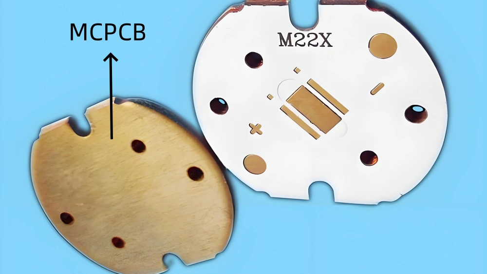
A copper core PCB uses a copper plate beneath or within its circuit construction. The metal carries heat away from a concentrated source and spreads it toward the cooling surface. The circuit copper, insulating dielectric and metal base each have a different job: routing current, providing electrical separation and carrying heat.
Part of the metal core PCB family, a copper-base board can be built around a simple insulated circuit or a more direct connection between a device thermal pad and the base.
Spread heat beyond the component footprint
Copper’s high thermal conductivity helps distribute heat from a small LED or power-device footprint over a larger area. This makes more of the base available to transfer heat into a heat sink or housing. The dielectric and the mounting interface remain important parts of that route; changing the base metal alone does not remove either interface.
Create the heat contact the assembly needs
Raised contacts, recessed regions and machined mounting features make the copper base more than a flat backing plate. A local copper contact can meet a suitable device thermal pad, while the surrounding insulated circuit carries its electrical connections. Copper surfaces can also be prepared for soldered joints where the product uses a soldered thermal or mechanical connection.
Bring the circuit and mounting arrangement together
The copper base supports the circuit and provides a rear cooling face. Fixing holes locate that face against the heat sink or housing; the outline fits the surrounding assembly. Shaped contact areas and mounting features let the board carry its circuit and its cooling connection in the same manufactured part.
Copper or aluminum?
Copper is useful when concentrated heat, a dedicated thermal contact or the joining arrangement justifies the material. Aluminum PCBs offer a lighter, generally lower-cost metal-base option for many lighting and driver products.
| Selection point | Copper base | Aluminum base |
|---|---|---|
| Heat spreading | Higher bulk metal conductivity; useful beneath concentrated heat sources | Effective heat spreading with a lower-weight base |
| Mechanical and thermal interfaces | Machined contact features and solderable surfaces can be integrated into the construction | Commonly used with mechanically fixed cooling faces and thermal interface materials |
| Weight and material cost | Heavier; the required material and machining contribute to cost | Lighter and usually less expensive for a comparable base |
Copper Core PCB Types and Stack-Ups
Choose the circuit arrangement and heat-transfer route together. The number of circuit layers describes routing capacity; thermal separation describes how a particular device contacts the base.
Scroll to compare constructions
| Construction | Circuit and base arrangement | Heat-transfer feature | Typical product needs |
|---|---|---|---|
| Single-sided insulated | A circuit layer over dielectric bonded to the copper base | Heat crosses the dielectric into the base | LED modules and power circuits with straightforward routing |
| Double-sided copper core | Circuits arranged around a copper core with insulated electrical connections where required | Combines routing on two sides with a metal heat-spreading structure | More interconnected power or lighting assemblies |
| Single-sided multilayer copper-base | Multiple circuit and dielectric layers built on the circuit side of a copper base | Supports more routing while retaining the copper cooling structure | Modules combining power, control and interconnect functions |
| Thermal-separation / DTP | A dedicated copper contact reaches a compatible device thermal pad; electrical pads remain insulated | The local heat contact bypasses the usual dielectric beneath that pad | High-power LEDs and devices with a suitable separate thermal interface |
Direct thermal path: change the route under the device
In an insulated board, heat travels from the device through its solder connection and the dielectric before reaching the copper base. A direct thermal path, or DTP, places a copper pedestal or contact beneath the device’s dedicated thermal pad. The surrounding electrical pads remain on the insulated circuit.
The contact replaces the dielectric beneath that particular thermal pad with a continuous copper route into the base. Its position and area follow the device footprint, and its height matches the surrounding circuit build so the electrical leads and thermal pad can be soldered together. The solder bond and base-to-heat-sink contact remain parts of the finished heat path.
The package’s thermal-pad electrical potential and its relationship to the base determine the appropriate contact arrangement. Heat then passes through the base and mounting interface into the cooling structure.

Copper Core PCB Design Options
The design defines the circuit, the thermal contact and the way the board fits its product. FLJ carries those choices into the substrate construction and fabrication details.
Dielectric and thermal contact
Dielectric thickness and thermal conductivity determine how readily heat crosses the insulating layer. With the same material and contact area, increasing thickness increases that layer’s thermal resistance. We select the dielectric with the required electrical separation and the available heat-transfer area, rather than treating conductivity as the only material property.
Where a direct contact is used, the thermal pad and copper pedestal are treated as a separate interface. We align the contact with the package and match its height to the adjacent dielectric and circuit build so the soldered device can seat correctly.
Electrical connections through a metal base
Mounting holes and electrical through-connections perform different tasks. An electrical passage through the conductive base needs an insulating separation between the circuit connection and the metal.
One construction forms a larger clearance in the core, fills it with insulation, then drills and plates a smaller electrical passage. This provides a conductive connection through the board while keeping it isolated from the base. The clearance and finished connection are defined with the selected construction.
Circuit copper and etched geometry
Circuit copper thickness is separate from copper-base thickness. The circuit carries current; its width, thickness and spacing are chosen for the electrical layout and fabrication process. Heavier circuit copper requires room for the etched geometry, reflected in our copper-dependent line and space capabilities below.
Local thermal contacts and their electrical clearances are developed with the circuit pattern. Our DFM and DFA review connects these features to the processes used to make and assemble the board.
Profiles, mounting faces and solderable pads
Slots, fixing holes, cut-outs and routed profiles locate the board in its assembly. Machined edges are deburred, and the rear contact face is kept suitable for its thermal interface and fixing arrangement.
The exposed pads receive a PCB surface finish selected for soldering, storage and the intended contact. Mask openings and any thermal-contact window are coordinated with the pad layout, giving the assembly process defined electrical and thermal joining areas.
Copper Core PCB Manufacturing and Assembly
FLJ supplies copper-base prototypes and production boards, including insulated and thermal-separation structures. Fabrication combines the selected circuit build with the shaped metal base and its thermal interfaces.
| Circuit layers | 1–8 |
|---|---|
| Product constructions | Single-sided, double-sided with core, single-sided multilayer and thermal separation |
| Finished board thickness | 0.5–5.0 mm |
| Finished circuit copper | 1–3 oz |
| Board size | 5 × 5 mm to 1200 × 480 mm |
| Minimum drilling hole | 0.6 mm |
| Line / space at 1 oz | 4 / 5 mil |
| Line / space at 2 oz | 6 / 8 mil |
| Line / space at 3 oz | 10 / 11 mil |
| Outline tolerance | CNC ±0.15 mm; punching ±0.1 mm |
Form the copper base and insulated circuit
For a pedestal-based construction, we form the copper relief and prepare matching openings in the dielectric and circuit layers. The layers are registered around the contact and bonded into the board. This produces a raised thermal contact beside an insulated electrical circuit, with the contact height carried through from the device and stack-up design.
Imaging and etching produce the circuit pattern. Drilling, routing and profile machining form the required holes, slots and outlines. The detailed sequence follows the construction, with the copper base protected during processing and handling.
Inspect the interfaces that matter
Circuit continuity and short-circuit checks are combined with the insulation checks applicable to the construction. Dimensional inspection covers holes, outlines and thermal-contact locations. Pad finish, contact surfaces and machined edges are also checked so the delivered board has solderable joining areas and a clean face for mounting against its cooling surface.
The metal core PCB capability tables give separate aluminum and copper ranges. Dimensions, circuit copper and feature geometry are matched within the chosen construction.
Supply the board with components assembled
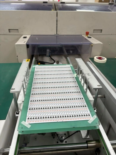
Copper-base fabrication can continue into PCB assembly, including component sourcing, placement and the inspection or testing needed for the product. This keeps the substrate, thermal-pad layout and assembly arrangement together from the first build through production.
The copper base changes how heat moves through the board during soldering. In SMT assembly, solder-paste deposition, board support and the measured reflow profile are matched to the assembled construction. The aim is a sound electrical joint and a well-wetted thermal contact beneath the device, followed by a clean, usable mounting interface.
Copper Core PCB Applications
Copper-base boards support products in which heat is concentrated in a small device area and must reach a larger cooling surface. The package, circuit and mounting arrangement determine the useful construction.
High-power LED modules
Spotlights, industrial luminaires and stage-lighting modules concentrate heat beneath one or several emitters. Copper spreads that heat toward the heat sink, while a compatible DTP construction provides a dedicated connection beneath the LED thermal pad. The mounting face, fixing pattern and optical arrangement remain coordinated with the light engine.
Automotive LED lighting
Headlamps and other compact LED light engines combine closely positioned emitters, defined optical alignment and a limited cooling space. A copper-base board can connect the local heat source to the lamp’s thermal structure. Routed outlines and fixing features locate the board, while the chosen electrical insulation and heat-contact arrangement follow the LED package and assembly.
Power conversion and industrial switching
Rectifier stages, converters and switching modules need to move heat from power devices into their cooling arrangement. Copper-base construction provides a heat spreader alongside the circuit and control connections. Circuit copper and conductor geometry address current carrying; the dielectric or dedicated thermal contact addresses the electrical and thermal relationship between the device and the base.
RF and communication power modules
Power-amplifier and transmitter modules combine a heat-generating active device with a defined RF signal path. In an appropriate copper-base or mixed-material construction, the copper spreads heat toward the chassis or heat sink, while the selected signal laminate and geometry provide the required RF circuit. High-frequency PCB materials and the thermal base perform complementary roles.
Request a Copper Core PCB Quote
Tell us about the board, device and cooling arrangement you want to build. FLJ can supply custom copper-base fabrication or an assembled board, with engineering support for the construction, mounting details and production quantities.