Bảng HDI Đáp ứng nhu cầu của các mạch tích hợp (IC) mật độ cao và lắp ráp kết nối mật độ cao. Chúng thúc đẩy Sản xuất bảng mạch in (PCB) Đưa lên một tầm cao mới. HDI là một trong những chủ đề nóng nhất trong sản xuất PCB. Những người làm CAM cho nhiều loại PCB đều đồng ý. Bo mạch điện thoại HDI trông phức tạp và mật độ đường dẫn cao. Sản xuất CAM khó khăn và khó hoàn thành nhanh chóng và chính xác. Đối mặt với nhu cầu của khách hàng về chất lượng cao và giao hàng nhanh, tôi đã không ngừng luyện tập và tổng kết. Tôi có một số kinh nghiệm. Tôi chia sẻ nó ở đây với các đồng nghiệp làm CAM.
Xác định SMD là điểm khó khăn đầu tiên trong CAM.
Trong quá trình sản xuất PCB, quá trình chuyển mẫu và ăn mòn sẽ ảnh hưởng đến mẫu cuối cùng. Do đó, trong quá trình sản xuất CAM, chúng ta phải điều chỉnh các đường dẫn và linh kiện SMD theo quy tắc chấp nhận của khách hàng. Nếu không định nghĩa SMD chính xác, một số pad SMD trên bảng mạch hoàn thiện có thể quá nhỏ.
Khách hàng thường thiết kế CSP 0.5 mm trên bo mạch điện thoại HDI. Kích thước pad là 0.3 mm. Một số pad CSP có lỗ vias ẩn. Lỗ vias ẩn có thể trùng với pad chỉ có kích thước 0.3 mm. Điều này khiến pad CSP và pad cho lỗ vias ẩn bị chồng chéo hoặc giao nhau. Trong trường hợp này, chúng ta phải cẩn thận để tránh sai sót.
Các bước cụ thể
- Đóng các lớp khoan tương ứng với các lỗ vias ẩn và lỗ vias chôn.
- Định nghĩa SMD.
- Sử dụng các chức năng popup Tìm kiếm Tính năng và Chọn Tham chiếu. Từ lớp trên cùng và lớp dưới cùng, tìm các pad có chứa các lỗ mù. Di chuyển các pad này lần lượt sang lớp T và lớp B.
- Trong cửa sổ chọn tham chiếu, trên lớp T (lớp chứa các pad CSP), chọn các pad tiếp xúc với lỗ mù (blind via) cách 0.3 mm và xóa chúng. Xóa các pad CSP trên lớp trên cùng có kích thước 0.3 mm trong khu vực CSP. Sau đó, dựa trên thiết kế của khách hàng về kích thước, vị trí và số lượng pad CSP, tạo pad CSP của riêng bạn và định nghĩa nó là SMD. Sao chép pad CSP sang lớp TOP và thêm pad tương ứng với lỗ mù trên lớp TOP. Thực hiện tương tự cho lớp B.
- Sử dụng tệp danh sách khách hàng để tìm các linh kiện SMD khác bị bỏ sót hoặc được định nghĩa quá nhiều lần.
So với phương pháp sản xuất thông thường, phương pháp này có mục tiêu rõ ràng và ít bước hơn. Phương pháp này có thể tránh được các thao tác sai sót và hoàn thành nhanh chóng và chính xác.
Việc loại bỏ các pad không hoạt động cũng là một bước đặc biệt đối với bảng mạch điện thoại HDI.
Lấy một bảng mạch HDI thông thường có 8 lớp làm ví dụ. Đầu tiên, loại bỏ các pad không hoạt động trùng khớp với các lỗ vias cho các lớp 2–7. Sau đó, loại bỏ các pad không hoạt động trùng khớp với các lỗ vias chôn ngầm cho các lớp 3–6 và các lỗ vias cho các lớp 2–7.
Các bước:
- Sử dụng hàm NFPRemoval để loại bỏ các pad trùng khớp với các lỗ không mạ trên các lớp trên và dưới.
- Đóng tất cả các lớp khoan trừ các lỗ xuyên qua. Chọn NFPRemoveUndrillRemoveUndrillLEDpads để loại bỏ các pad không chức năng cho các lớp 2–7.
- Đóng tất cả các lớp khoan trừ các lỗ khoan chìm cho các lớp 2–7. Chọn NFPRemoveUndrilledPads và chọn NO để xóa các pad không hoạt động cho các lớp 3–6.
Sử dụng phương pháp này để loại bỏ các miếng đệm không hoạt động là đơn giản và dễ học. Phương pháp này phù hợp nhất cho những người mới bắt đầu làm việc với CAM.

Về khoan laser
Các lỗ mù trên bảng mạch điện thoại HDI thường là các lỗ vi mạch có đường kính khoảng 0,1 mm. Công ty chúng tôi sử dụng tia laser CO₂. Các vật liệu hữu cơ hấp thụ tia hồng ngoại mạnh và vật liệu bị bốc hơi do nhiệt để tạo lỗ. Tuy nhiên, đồng hấp thụ tia hồng ngoại ít và điểm nóng chảy của đồng cao. Tia laser CO₂ không thể bốc hơi lớp đồng. Do đó, đồng tại vị trí lỗ laser được loại bỏ bằng dung dịch ăn mòn. CAM phải tạo bản vẽ phơi sáng lỗ khoan cho mục đích này. Đồng thời, để đảm bảo lớp ngoài thứ hai (đáy của lỗ laser) giữ được đồng, khoảng cách giữa các lỗ mù và lỗ chôn phải ít nhất 4 mil. Do đó, chúng tôi phải sử dụng Phân tích / Sản xuất / Kiểm tra lỗ khoan trên bảng mạch để phát hiện các lỗ hỏng.
Qua quá trình hàn và lớp phủ hàn
Trong các lớp lamination HDI, các lớp ngoài thứ cấp thường sử dụng vật liệu RCC. Độ dày lớp cách điện mỏng và hàm lượng nhựa thấp. Các thử nghiệm quy trình cho thấy quy tắc sau: nếu độ dày bảng mạch hoàn thiện vượt quá 0.8 mm, và túi kim loại hóa có kích thước ≥ 0.8 mm × 2.0 mm, và lỗ kim loại hóa có kích thước ≥ 1.2 mm, thì chúng ta phải chuẩn bị hai bộ tệp điền lỗ. Tức là việc điền lỗ được chia thành hai lần điền. Các lớp trong được làm phẳng bằng nhựa, và lớp ngoài được điền bằng mực mặt nạ hàn trước bước mặt nạ hàn.
Trong quá trình phủ lớp chống hàn, các lỗ vias đôi khi nằm trên hoặc gần các pad SMD. Khách hàng yêu cầu tất cả các lỗ vias phải được lấp đầy. Do đó, các lỗ vias bị lộ ra ngoài hoặc chỉ lộ một phần trong lớp phủ chống hàn có thể dễ dàng gây ra hiện tượng keo hàn hoặc dầu mỡ bám trên pad. Nhân viên CAM phải xử lý tình huống này. Thông thường, chúng ta sẽ chọn cách mở lỗ vias. Nếu không thể di chuyển lỗ vias, hãy thực hiện các bước sau:
- Thêm một chấm cho phép ánh sáng xuyên qua trên lớp phủ hàn, có kích thước nhỏ hơn 3 mil ở một bên so với lỗ hoàn thiện.
- Thêm một chấm cho phép ánh sáng xuyên qua trên lớp phủ hàn, có kích thước lớn hơn 3 mil ở một bên so với lỗ hoàn thiện. (Trong trường hợp này, khách hàng cho phép một phần nhỏ của pad bị che phủ bởi lớp phủ.)
Tạo khung viền bảng và phân chia bảng thành các panel
Bo mạch điện thoại HDI thường được giao dưới dạng bảng mạch. Thiết kế phức tạp và khách hàng cung cấp file CAD cho việc chia bảng mạch. Nếu chúng ta vẽ bảng mạch sử dụng file của khách hàng với Genesis2000, việc này sẽ gặp nhiều khó khăn. Chúng ta có thể nhấp vào "Save As" trong tệp và thay đổi loại tệp lưu thành AutoCAD R14 / LT98 / LT97 DXF (*.DXF). Sau đó, chúng ta đọc tệp *.DXF như một tệp Gerber thông thường. Trong quá trình đọc đường viền, chúng ta cũng đọc kích thước và vị trí của các lỗ đóng dấu, lỗ định vị và các điểm tham chiếu quang học. Cách này nhanh chóng và chính xác.
Xử lý khung gia công
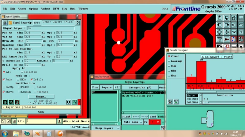
Khi gia công khung mạch, trừ khi khách hàng yêu cầu lộ đồng trong CAM, chúng tôi sẽ cắt một lượng nhỏ đồng vào trong khung để tránh tình trạng đồng ở mép bảng bị bong tróc trong quá trình sản xuất. Điều này có thể dẫn đến các trường hợp như Hình 2A. Nếu hai đầu của A không thuộc cùng một mạng và độ rộng đồng nhỏ hơn 3 mil (có thể không thể sản xuất được), thì sẽ gây ra tình trạng mở mạch. Phân tích Genesis2000 sẽ không hiển thị vấn đề này. Vì vậy, chúng ta phải sử dụng phương pháp khác. Chúng ta có thể thực hiện so sánh mạng nhiều lần hơn, và trong lần so sánh thứ hai, cắt đồng của khung vào bảng mạch. Nếu kết quả so sánh không hiển thị mạch hở, thì hai đầu của A thuộc cùng một mạng hoặc độ rộng lớn hơn 3 mil và mẫu có thể sản xuất được. Nếu có mạch hở, hãy mở rộng đồng.
Tóm tắt ngắn gọn các điểm chính
- Xác định SMD một cách cẩn thận. Sử dụng các công cụ đóng lớp và công cụ popup để tìm các pad chứa các lỗ vias ẩn. Thay thế các pad nhỏ bằng các pad CSP chính xác và sao chép lên các lớp trên và dưới. Điều này giúp tránh trùng lặp và lỗi.
- Loại bỏ các miếng đệm không hoạt động từng bước một bằng các công cụ loại bỏ NFP. Điều này rõ ràng và phù hợp cho nhân viên CAM mới.
- Đối với gia công laser, cần lưu ý rằng tia laser CO₂ không thể loại bỏ đồng. Sử dụng phương pháp ăn mòn và tạo bản vẽ phơi sáng cho lỗ khoan. Giữ khoảng cách tối thiểu 4 mil giữa các lỗ vias ẩn và chôn, đồng thời thực hiện kiểm tra lỗ khoan trên bảng mạch.
- Tạo lỗ vias bằng cách điền file khi độ dày bảng mạch và kích thước lỗ đáp ứng quy tắc. Chia lỗ vias bên trong và bên ngoài khi cần thiết. Xử lý lỗ vias gần các linh kiện SMD trong lớp phủ hàn bằng cách thêm các chấm cho phép ánh sáng xuyên qua.
- Để đọc file DXF cho bảng mạch, hãy chuyển đổi file CAD sang định dạng DXF và đọc nó như file Gerber để nhanh chóng và chính xác lấy được đường viền, lỗ đục và vị trí tham chiếu.
- Đối với khung đồng trong quá trình gia công, hãy kiểm tra các mạch và mở rộng đồng nếu so sánh cho thấy có khe hở.
Phương pháp này có mục tiêu rõ ràng và ít bước hơn. Sử dụng nó để giảm thiểu sai sót và tăng tốc quá trình sản xuất CAM chính xác cho bảng mạch điện thoại HDI.