
Layer-selective interconnections
Blind & Buried Via
PCB Manufacturing
Connect the layers your circuit needs. FLJ manufactures multilayer PCBs with blind and buried vias, combining mechanical and laser hole formation with the sub-board processing, copper metallization and lamination needed for the selected construction.
From prototype boards to production quantities, our fabrication service carries the via arrangement through engineering, manufacture and finished-board inspection.
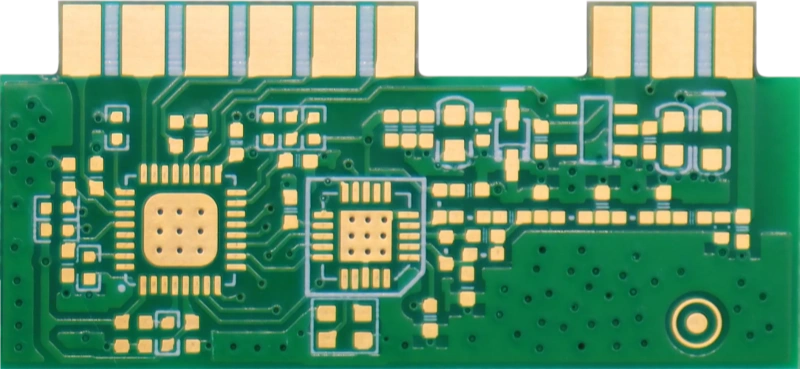
Request a PCB quoteCircuit-board detail · FLJ media library
Make room for the next connection
Blind, Buried and Through Connections
A blind via connects an outer copper layer to an inner layer without passing through the complete board. A buried via connects internal layers and has no opening on either finished surface. Both can leave other parts of the stack available for routing.
The hole occupies a span. The copper defines the net.
A through via passes through the full board thickness, but it does not have to connect electrically to every copper layer along the way. Capture lands connect the intended layers to the plated wall; clearances keep other copper isolated.
A blind connection can take a surface signal down to a nearby routing layer. A buried connection can move between internal layers while leaving the surface regions above and below it unpierced. The layer span and its pads are selected together.
High-I/O processors, FPGAs and compact communication modules benefit when a dense pad field can reach internal routing without a full-depth hole occupying every layer. The broader multilayer construction still establishes the signal, power and reference layers around those connections.
| Connection | Access in the finished board | Depth relevant to fabrication | Routing effect |
|---|---|---|---|
| Through via | Both board faces | The complete board thickness | A drilled path across the stack, with clearances on non-connected layers |
| Blind via | One outer face | The selected surface-to-inner-layer span | Leaves deeper layers free of this drilled path |
| Buried via | Neither outer face | The internal sub-board processed for that connection | Leaves regions outside the internal span available for other features |
Manufacture the connection before it disappears inside the stack
How Blind and Buried Vias Are Manufactured
The finished via name describes where the connection ends. Its manufacturing route also depends on which part of the board is accessible when drilling and copper deposition take place. FLJ coordinates the via groups with the cores, bonding layers and lamination stages.
Buried vias: process the internal sub-board first
The required cores or laminated sub-board carry the internal circuitry and the lands that the buried connection will join. FLJ registers the hole pattern to that structure, drills the specified span and prepares the exposed hole surfaces for metallization.
The freshly drilled hole contains insulating resin and reinforcement as well as exposed copper. A conductive seed layer allows subsequent copper deposition to build the plated wall. That wall must meet the intended internal lands to form a continuous electrical path.
When the connection and applicable internal checks are complete, the remaining layers are bonded around the sub-board. A hole that passed through the processed sub-board is now buried inside the finished PCB. Filling and surface preparation are included where the selected construction calls for them.
L3–L6 accessible
Connection enclosed

Blind vias: reach the target from the selected face
A blind connection can be produced through an appropriate controlled-depth process or by processing an accessible core or sub-board before the rest of the stack is added. In a core-first route, the hole is drilled and plated while the copper-clad core remains a separate board. Keeping one end at the eventual outer surface makes that connection blind in the finished stack.
The core and bonding-layer positions matter. A span across a bonding interface cannot be made simply by drilling the loose prepreg as though it were a cured board. It needs a suitable processed sub-board, build-up or depth-controlled route. Mechanical drilling and laser processing are selected with that physical construction.
Controlled-depth mechanical drilling reaches the defined inner connection while preserving the intended separation from deeper features. Laser processing creates a shallow opening through the selected build-up dielectric to its landing copper. The entry geometry, material removal and target surface are parts of the same connection.
Residue at the bottom can prevent deposited copper from bonding to the landing. Hole preparation therefore follows the material and formation method. Wetting and solution exchange also matter: copper must reach the recessed surfaces, rather than merely accumulate at the opening.
Laser microvias and sequential build-up can be incorporated into an HDI PCB construction. Blind and buried describe connection access; microvia adds a particular geometry and construction category.
Geometry and fabrication options
FLJ combines the hole route, processed depth and capture lands with the spacing needed by neighboring copper. Depth-to-diameter ratio uses the depth actually being processed, divided by the hole diameter. A recessed blind hole and a hole drilled through an internal sub-board have different access for cleaning and copper deposition, even when they become parts of the same finished PCB.
For the buried connection, the relevant drilling thickness is the processed sub-board. For a hole cut from one face, it is the selected cut depth. Applying the whole finished-board thickness to either feature can misdescribe the actual process geometry.
| Tính năng | FLJ reference | Đơn đăng ký |
|---|---|---|
| Mechanical blind / buried vias, same net | 10 mil hole-wall spacing | Edge-to-edge wall distance for the same-net mechanical blind / buried condition |
| Laser vias, same net | 6 mil hole-wall spacing | A separate spacing reference from mechanical blind / buried holes |
| Holes on different nets | 10 mil after compensation | Hole-wall clearance for the different-net condition |
| Laser hole & capture pad | 4 / 10 mil 5 / 11 mil | Hole diameter / pad diameter pairings |
| Laser build-up stages | 1–5 | Matched to the via sequence, dielectric and lamination plan |
1 mil = 0.0254 mm. Laser hole/pad figures are paired references. The PCB manufacturing capability reference covers the wider fabrication scope.
Capture-pad selection leaves copper around the finished hole after registration and process allowances. Hole-wall spacing measures the gap between the hole edges, rather than the distance between drill centres. Keeping drill diameter, finished hole, pad and processed depth distinct makes the via schedule usable in manufacture.
Choose the work that opens the routing path
Routing Choices, Build Complexity and Cost
The useful construction is the one that makes the required connection within the available board area. An added via level creates value when it opens a needed route.
Surface escape
A blind connection can move a net away from a fine-pitch pad field into an inner routing layer. The pad pattern, usable channels and reference copper determine how much space that saves. A via within an assembly pad also needs the appropriate filling and finished land surface.
Internal interconnection
A buried span links the chosen internal layers without opening either finished surface. It can preserve the surface region for components and other routing, while adding drilling, metallization and possibly another lamination stage to the internal build.
Unused through-via length
If the issue is an unused plated stub rather than routing space, a through via with backdrilling may suit the signal path. Backdrilling removes unwanted barrel copper after plating; it is a different operation from making a new blind connection. See high-speed PCB fabrication for the channel and stub relationship.
Quote the complete construction
The number of processed sub-boards, hole-formation and plating operations, lamination cycles, material system, filling and inspection contribute to cost. Total copper-layer count alone does not describe that work. A deeper span may change the manufacturing route even when the finished outline stays the same.
Fewer occupied routing regions can improve layout flexibility, but do not automatically mean fewer copper layers or a lower finished-board price. FLJ develops the fabrication proposal around the actual layer connections, board geometry and order quantity.
Inspect the copper path, not just the finished surface
Inspecting the Internal Copper Connection
A finished board hides the buried hole and much of the blind connection. Inspection therefore follows the structure through manufacture: accessible internal patterns before enclosure, hole registration and deposited copper at the appropriate process stages, and the electrical network after fabrication.
Registration, interfaces and thermal exposure
The drilled path must reach the intended capture lands. Hole preparation exposes the copper surfaces that the deposit must join, while plating forms the conductive wall or specified filled structure. Registration, surface condition and deposited copper all contribute to the same interconnect.
Later lamination and assembly heat act on connections already inside the board. Expansion of the substrate and copper can load those interfaces. The material system and fabrication route are selected for that thermal history; qualification uses representative structures and the conditions relevant to the application.
Examine accessible internal copper and the registered structures before the remaining layers cover them.
A section through the selected feature exposes the blind-hole landing and its deposited-copper interface, or the buried barrel where it joins an internal land. Section position follows the interface being examined.
Bare-board electrical testing checks continuity and isolation against the intended circuit.
A cross-section and a continuity check provide different evidence. Initial continuity does not by itself establish performance through long-term thermal stress. Where further qualification is needed, its specimen, exposure and acceptance conditions are defined for the construction.
FLJ supplies the fabricated boards and can continue into BGA PCB assembly, connecting the finished lands to component placement, soldering and hidden-joint inspection.
Request a blind & buried via PCB quote
Send your available fabrication files, layer stack, via spans and quantities. Include any particular material, filling or inspection needs so the quotation covers the connection you want manufactured.