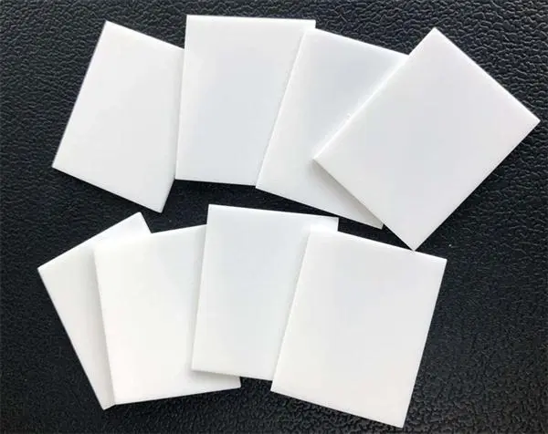
الركيزة السيراميكية هي نوع خاص من الألواح المصنوعة عن طريق ربط رقائق النحاس مباشرة بسطح أكسيد أو لوح سيراميك عند درجة حرارة عالية. يتم ربط النحاس بالسيراميك من خلال عملية درجة حرارة عالية بحيث يشكل المعدن والسيراميك قاعدة ثابتة للدوائر.
a. لها قوة ميكانيكية عالية. يمكنها حمل الأجزاء وتعمل أيضاً كهياكل داعمة.
b. يسهل تشغيلها آلياً. تحتفظ بأبعاد دقيقة. يمكن تصنيعها في عدة طبقات.
c. سطحها أملس. لا تلتوي أو تنحني أو تظهر عليها شقوق صغيرة.
a. لديها مقاومة عزل عالية وجهد انهيار عالٍ. وهذا يحافظ على سلامة الدوائر من التقصير ومن تلف الجهد العالي.
b. لديها ثابت عازل كهربائي منخفض وفقدان عازل كهربائي منخفض. وهذا يساعد على تمرير الإشارات بفقد أقل.
c. يبقى أداؤها مستقرًا في درجات الحرارة العالية والرطوبة العالية. وهذا يساعد على ضمان الموثوقية في ظروف الاستخدام الصعبة.
a. لديها موصلية حرارية عالية. وهذا يساعد على نقل الحرارة بعيدًا عن الأجزاء الساخنة.
b. يمكن أن يتطابق معامل تمددها الحراري مع المواد ذات الصلة، وخاصة السيليكون. يقلل هذا التطابق من الإجهاد عند تسخين الأجزاء وتبريدها.
c. تتمتع بمقاومة جيدة للحرارة. تظل مستقرة في درجات الحرارة العالية.
a. مستقرة كيميائياً. يسهل تمعدنها. تلتصق بها أنماط الدوائر بشكل جيد.
b. لا تمتص الرطوبة. تقاوم الزيت والهجوم الكيميائي. تطلق القليل من الإشعاع.
c. المواد المستخدمة غير ضارة وغير سامة. لا يتغير تركيبها البلوري في نطاق درجة حرارة العمل.
d. المواد الخام وفيرة. التكنولوجيا ناضجة. وهي سهلة الصنع وسعرها منخفض.
قبل إطلاق السيراميك، هناك أربع طرق تشكيل شائعة قبل التشكيل. وهي كبس المسحوق (الذي يمكن أن يكون كبس القالب أو الكبس المتساوي الضغط)، والبثق، وصب الشريط، والقولبة بالحقن. من بين هذه الطرق، غالبًا ما يتم استخدام صب الشريط في السنوات الأخيرة لحزم LSI وركائز الدوائر الهجينة لأنه من الأسهل صنع العديد من الطبقات ولديه كفاءة إنتاج أعلى.
مسارات العملية الشائعة هي هذه الثلاثة:
- تكديس الطبقات - الكبس الساخن - إزالة الغلاف - إطلاق اللوح الأساسي - تشكيل أنماط الدائرة - إطلاق الدائرة.
- تكديس الطبقات - طباعة نمط الدائرة على السطح - الكبس الساخن - إزالة الغلاف - إطلاق النار المشترك.
- طباعة نمط الدائرة الكهربائية - الرص - الكبس الساخن - إزالة الغلاف - الإشعال المشترك.
في طريقة الغشاء السميك، يتم تشكيل الموصلات (آثار الدائرة) والمقاومات على السيراميك عن طريق طباعة الشاشة. بعد الطباعة، يتم تلبيد الأجزاء لتشكيل الدائرة الكهربية ووسادات التلامس. تشمل المواد اللاصقة المستخدمة لتثبيت المعدن المطبوع نوع الزجاج ونوع الأكسيد وأنواع الأكسيد الزجاجي والأكسيد المختلط.
تستخدم الأغشية الرقيقة طرق تفريغ الهواء مثل التبخير أو الطلاء بالأيونات أو الرش لتطبيق المعدن. ولأن الغشاء الرقيق يرسب المعدن من المرحلة الغازية، يمكن من حيث المبدأ ترسيب أي معدن. كما يمكن من حيث المبدأ تمعدن أي ركيزة بهذه الطريقة. ولكن يجب أن يتطابق التمدد الحراري للفيلم المعدني والركيزة الخزفية قدر الإمكان. ومن المهم أيضًا زيادة التصاق الطبقة المعدنية بالسيراميك.
قبل الحرق، تُطبع معاجين معدنية حرارية من المونيوم والوايت والمعادن المماثلة على صفائح السيراميك غير المحروقة. ثم يتم بعد ذلك إزالة الرقائق وحرقها بحيث يشكّل السيراميك والمعدن بنية واحدة متكاملة. تتميز هذه الطريقة بهذه الميزات:
■ يمكن أن تشكل خطوط دارة دقيقة للغاية ومن السهل صنع العديد من الطبقات، لذا فإن الأسلاك عالية الكثافة ممكنة.
■ نظرًا لتكوين العازل والموصل معًا، فإن الختم المحكم في العبوات ممكن.
■ باختيار التركيبة الصحيحة وضغط التشكيل ودرجة حرارة التلبيد المناسبة، يمكن التحكم في انكماش التلبيد. خاصةً عندما يتم تصنيع ركيزة ذات انكماش صفري في المستوى، وهذا يفتح المجال لاستخدامها في BGA وCSP والتغليف عالي الكثافة للرقاقة العارية.
a. مادة خام: Al₂O₃O₃ غالبًا ما يتم تصنيعها بواسطة
عملية باير. في هذه الطريقة، تكون المادة الخام هي البوكسيت الذي يتضمن أكاسيد الألومنيوم المطفأ والمركبات ذات الصلة.
b. الصنع: عادةً ما يتم تشكيل سيراميك Al₂O₃O₃ من خلال تكديس صفائح غير مشتعلة. وغالبًا ما يتم استخدام مادة رابطة مثل البولي فينيل بوتيرال (PVB). وتختلف درجة حرارة الحرق مع إضافة مساعدات التلبيد، وعادةً ما تكون 1550-1600 درجة مئوية. وتتمثل طرق معدنة الأل₂O₃O↩O₃ بشكل أساسي في طرق الحرق المشترك والأغشية السميكة. وتعتبر المعاجين وتكنولوجيا المعالجة ناضجة. وهي تلبي العديد من احتياجات التطبيق اليوم.
c. التطبيقات: ركائز للدوائر المتكاملة الهجينة، وركائز حزم الدوائر المتكاملة الهجينة، وركائز الدوائر متعددة الطبقات.
الموليت هو أحد أكثر الأطوار البلورية استقرارًا في نظام Al₂O₃-SiO₂. بالمقارنة مع Al₂O₃O₃، يتميز الموليت بقوة ميكانيكية أقل قليلاً وموصلية حرارية أقل، ولكن ثابت العزل الكهربائي الخاص به أقل. يمكن أن يساعد ثابت العزل الكهربائي المنخفض هذا في تحسين سرعة الإشارة. كما أن معامل التمدد الحراري الخاص به منخفض، مما يقلل من الضغط الحراري على LSI المركب. كما أن فرق التمدد مع المعادن الموصلة مثل Mo وW أصغر، لذا فإن الحرق المشترك يسبب ضغطًا أقل بين المعدن والسيراميك.
a. المادة الخام: ألن ليس معدنًا طبيعيًا. إنها مادة من صنع الإنسان تم تصنيعها لأول مرة في القرن التاسع عشر. تُصنع مساحيق AlN النموذجية عن طريق الاختزال بالنتريد الاختزالي أو النتريد المباشر. وتبدأ طريقة الاختزال بالنتريد الاختزالي من Al₂O₃O₃ وتستخدم الكربون عالي النقاء لاختزاله، ثم يتفاعل مع النيتروجين لتكوين Al₂N. أما طريقة النتريد المباشر فتتفاعل مسحوق الألومنيوم مع N₂ لتكوين AlN مباشرةً.
b. الصنع: يمكن استخدام نفس طرق التشكيل المستخدمة لركائز Al₂O₃O₃ لـ Al₂N. والطريقة الأكثر استخدامًا هي تكديس الصفائح غير المشتعلة. لهذا الغرض، يتم خلط مسحوق AlN، والمواد العضوية الرابطة والمذيبات والمادة الخافضة للتوتر السطحي لصنع ملاط خزفي. يتم صب الملاط على شريط لاصق، وتكديسه، وضغطه على الساخن، وإزالة الرغوة منه، ثم حرقه لصنع ركيزة AlN.
c. ميزات الركيزة AlN: يتميز AlN بتوصيل حراري يزيد عن عشرة أضعاف توصيل Al₂O₃O₃. يتطابق معامل تمددها الحراري (CTE) مع السيليكون. بالمقارنة مع Al₂O₃، تتمتع AlN بمقاومة عزل أعلى وجهد انهيار أعلى. ثابت العزل الكهربائي أقل. هذه الميزات تجعل من AlN قيمة للغاية بالنسبة لركائز الحزمة.
d. التطبيقات: تُستخدم لوحدات مضخمات الطاقة ذات النطاق الترددي العالي جداً، والأجهزة عالية الطاقة، وركائز الصمام الثنائي الليزري.
a. مادة خام: SiC ليس معدنًا طبيعيًا. يتم تصنيعه عن طريق خلط السيليكا وفحم الكوك وقليل من الملح كمساحيق. يتم تسخين المزيج في فرن جرافيت فوق 2000 درجة مئوية للتفاعل وتكوين α-SiC. ثم يمكن تنقية SiC عن طريق التسامي للحصول على كتلة خضراء داكنة من مادة متعددة البلورات.
b. الصنع: يتميز SiC بثبات كيميائي وحراري عالٍ للغاية، لذا فإن طرق الحرق العادية تجعل من الصعب تكثيفه. هناك حاجة إلى مساعدات التلبيد وطرق الحرق الخاصة. يشيع استخدام الكبس الساخن بالتفريغ.
c. ميزات SiC: الميزة الرئيسية هي معامل الانتشار الحراري الكبير جداً. ويمكن أن يكون أكبر من النحاس. تمدده الحراري أقرب إلى السيليكون. ولكن لدى SiC بعض الجوانب السلبية. ثابت العزل الكهربائي الخاص به مرتفع نسبيًا وجهد الانهيار ليس جيدًا مثل بعض أنواع السيراميك الأخرى.
d. التطبيقات: تُستخدم ركائز SiC حيثما تكون هناك حاجة إلى انتشار الحرارة العالية والجهد غير مرتفع. وهي تستخدم في حزم التغريق الحراري VLSI، و LSI المنطقية عالية السرعة وعالية التكامل مع المشتتات الحرارية، وأجهزة الكمبيوتر الكبيرة، وركائز الصمام الثنائي الليزري للاتصالات البصرية.
يتميز BeO بتوصيل حراري يعادل عدة أضعاف توصيل Al₂O₃O₃. يعمل بشكل جيد للدوائر عالية الطاقة. ثابت العزل الكهربائي الخاص به منخفض، لذا فهو مناسب للدوائر عالية التردد. عادةً ما تُصنع ركائز BeO بالضغط الجاف. كما يمكن تصنيعها أيضًا عن طريق الصفائح غير المشتعلة بإضافات صغيرة من MgO أو Al₂O₃O₃. ونظرًا لأن مسحوق أكسيد البولي أوكسيد الفوسفات سام، فإن منتجات أكسيد البولي أوكسيد الفوسفات تثير مخاوف بيئية وصحية. في اليابان لا يُسمح بإنتاج ركيزة أكسيد البولي أوكسيد الفوسفات في اليابان ويجب استيراد أكسيد البولي أوكسيد الفوسفات من أماكن مثل الولايات المتحدة.
من الهيكل وطرق التصنيع، يمكن تجميع ركائز السيراميك في HTCC، LTCC، TFC، DBC، DPC، DPC، وما إلى ذلك. يتم استخدام ركائز السيراميك أكثر فأكثر في التغليف الإلكتروني وفي إلكترونيات الطاقة مثل IGBT (ترانزستور ثنائي القطب معزول البوابة)، و LD (الصمام الثنائي القطب)، و LED عالي الطاقة، و CPV (الكهروضوئية المركزة) بسبب الموصلية الحرارية الجيدة، ومقاومة الحرارة، والعزل، والتمدد الحراري المنخفض، وانخفاض التكلفة.
المواد الأساسية الخزفية الشائعة هي BeO، وAl₂O₃، وAlN، وSi₃N₄. من بين هذه المواد، يتميز Si₃N₄N₄ بعزل كهربائي عالٍ جدًا واستقرار كيميائي. كما أنها تتمتع بثبات حراري جيد وقوة ميكانيكية عالية. يمكن استخدامه للوحات الدوائر الكهربائية عالية الكثافة والتكامل العالي.
HTCC عبارة عن ركيزة خزفية ذات درجة حرارة عالية يتم حرقها بشكل مشترك. ولصنع HTCC، يتم أولاً خلط مسحوق السيراميك مثل Al₂O₃ أو AlN مع مادة رابطة عضوية. يُصنع المزيج في عجينة ثم يتم تشكيله في صفائح بواسطة شفرة الطبيب أو طرق مماثلة. تصبح الصفائح المجففة أجسامًا خضراء. يتم حفر الثقوب الخاصة بالفتحات ويتم طباعة معاجين الموصلات على الشاشة لتوصيل الأسلاك وتعبئة الفتحات. ثم يتم تكديس الصفائح الخضراء ووضعها في فرن بدرجة حرارة عالية حوالي 1600 درجة مئوية للتلبيد. نظرًا لأن درجة حرارة التلبيد عالية، فإن اختيار المعادن الموصلة محدود. يتم استخدام معادن ذات نقاط انصهار عالية ولكن ذات توصيل أقل، مثل التنجستن والموليبدينوم والمنجنيز. التكلفة عالية والتوصيل الحراري يتراوح تقريبًا بين 20-200 واط/(م-درجة مئوية).
سيراميك LTCC عبارة عن سيراميك منخفض الحرارة يتم حرقه في درجة حرارة منخفضة. وتتشابه خطوات صنعه مع سيراميك HTCC. ويكمن الفرق في أن مسحوق Al₂O₃O₃ يتضمن 30-50% من الزجاج منخفض درجة الانصهار. وهذا يخفض درجة حرارة الحرق إلى حوالي 850-900 درجة مئوية. ونظرًا لانخفاض درجة حرارة الحرق، يمكن استخدام المعادن الموصلة ذات الموصلية الجيدة مثل الذهب والفضة للأقطاب الكهربائية والآثار. يستخدم LTCC طباعة الشاشة للخطوط المعدنية. يمكن أن يكون لهذه الطريقة أخطاء في المحاذاة بسبب تمدد الشبكة. كما يمكن أن يحدث انكماش مختلف عند تكديس الطبقات المتعددة وإطلاقها بشكل مشترك، مما يضر بالإنتاجية. ولرفع التوصيل الحراري لطبقات LTCC، يمكن إضافة فيات حرارية أو فيات موصلة في مناطق المكونات، ولكن ذلك يرفع التكلفة.
وبالمقارنة مع LTCC وHTCC، فإن TFC عبارة عن ركيزة سيراميك بعد الحرق. وهي تستخدم طباعة الشاشة لتطبيق المعاجين المعدنية على سطح القاعدة الخزفية. بعد التجفيف، يتم حرق الجزء عند درجة حرارة عالية (700-800 درجة مئوية). تُصنع المعاجين المعدنية من مسحوق معدني وراتنج عضوي وزجاج. بعد الحرق، يحترق الراتنج وتتكون الطبقة المتبقية في الغالب من معدن مرتبط بمادة لاصقة زجاجية على سطح السيراميك. يبلغ سمك الطبقة المعدنية المحروقة عادةً 10-20 ميكرومتر ويبلغ الحد الأدنى لعرض الخط حوالي 0.3 مم. ولأن التكنولوجيا ناضجة والعملية بسيطة والتكلفة منخفضة، يتم استخدام TFC حيثما لا تكون احتياجات دقة النمط عالية.
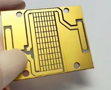
تُصنع DBC عن طريق التلبيد المشترك أو الربط سهل الانصهار لرقائق النحاس بصفائح السيراميك عند درجة حرارة عالية (حوالي 1065 درجة مئوية). بعد الربط، يتم تشكيل أنماط الدوائر الكهربائية عن طريق الحفر. ونظرًا لأن رقائق النحاس لديها توصيل كهربائي وحراري جيد ويمكن لرقائق النحاس أن تتحكم في تمدد مركب النحاس-أل-أو-أو-نحاس-نحاس-نحاس مركب، فإن DBC لديها تمدد حراري قريب من تمدد الألومينا. يتميز DBC بتوصيل حراري جيد، وعزل قوي، وموثوقية عالية. ويستخدم على نطاق واسع في IGBT، والصمام الثنائي الليزري، والتغليف الكهروضوئي المركزي. DBC له عيوب. يحتاج التفاعل سهل الانصهار ذو درجة الحرارة العالية بين النحاس وأكسيد الألومنيوم إلى تحكم صارم في المعدات والعملية، وبالتالي فإن التكلفة أعلى. يمكن أن تتشكل مسام دقيقة بين Al₂O₃ والنحاس، مما يقلل من مقاومة الصدمات الحرارية. يمكن أن تتشوه رقائق النحاس عند درجة حرارة عالية، لذلك عادةً ما يكون سمك النحاس على DBC أكثر من 100 ميكرومتر. كما يُستخدم الحفر أيضًا لتشكيل الأنماط، لذلك يكون الحد الأدنى لعرض الخط عادةً أكثر من 100 ميكرومتر.

يبدأ DPC بالتنظيف والمعالجة المسبقة لصفائح السيراميك. ثم يتم ترسيب طبقة أولية من Ti/Cu عن طريق الرش بالتفريغ على سطح الركيزة. يتم استخدام الطباعة الليثوغرافية الضوئية والتطوير والحفر لتشكيل نمط الدائرة. ثم يُستخدم الطلاء الكهربائي أو الطلاء الكيميائي لزيادة سُمك الدائرة. بعد إزالة مقاوم الضوء تكتمل الركيزة. وتتميز الطباعة الليثوغرافية الضوئية بما يلي: عملية ذات درجة حرارة منخفضة (أقل من 300 درجة مئوية)، وبالتالي فهي تتجنب عيوب ارتفاع درجة الحرارة للمواد والدوائر وتقلل من تكلفة التصنيع. استخدام طبقة رقيقة وطباعة ليثوغرافية ضوئية تجعل الخطوط المعدنية على الركيزة أدق. لذا فإن DPC مناسب تمامًا للحزم التي تحتاج إلى دقة محاذاة عالية. لكن DPC له سلبيات أيضًا. فسمك النحاس المطلي بالكهرباء محدود، ويمكن أن يتسبب سائل نفايات الطلاء الكهربائي في حدوث تلوث. كما أن الالتصاق بين الطبقة المعدنية والسيراميك أقل، لذلك قد تكون موثوقية المنتج أقل.
عند اختيار الركيزة الخزفية، قم بمطابقة المادة مع احتياجات التطبيق. إذا كنت بحاجة إلى موصلية حرارية عالية وتمدد حراري قريب من السيليكون، فقد يكون AlN أو SiC هو الأفضل. إذا كانت التكلفة والمعالجة الناضجة مهمة، فإن Al₂O₃O₃ خيار قوي. إذا كنت بحاجة إلى خطوط دقيقة ومعالجة بدرجة حرارة منخفضة، فيمكن أن تعمل DPC وLTCC. أما إذا كنت بحاجة إلى أسلاك متعددة الطبقات عالية الكثافة ومُحكمة الإغلاق، فقد تكون الطرق التي يتم إطلاقها بشكل مشترك مثل LTCC أو HTCC مع المعدن الملبد المشترك هي الخيار المناسب.
تشمل مجالات التطبيق الشائعة وحدات الطاقة ومضخمات طاقة الترددات اللاسلكية ووحدات الصمام الثنائي الليزري ومصابيح LED عالية الطاقة وتغليف LSI عالي الكثافة. تستفيد إلكترونيات الطاقة من ركائز السيراميك لأنها تنقل الحرارة بشكل جيد وتحافظ على العزل والقوة الميكانيكية تحت الضغط الحراري. تستفيد أجهزة الترددات اللاسلكية من الفقد العازل المنخفض وخصائص العزل الكهربائي المستقرة. تكتسب العبوات عالية الكثافة من القدرة على عمل خطوط دقيقة وتكديس العديد من الطبقات مع التحكم الجيد في المحاذاة إذا كانت العملية مناسبة.
كل نوع سيراميك وكل عملية لها مقايضات. يستخدم HTCC درجة حرارة حرق عالية وبالتالي يستخدم معادن حرارية للموصلات. وهذا يحد من التوصيل ويرفع التكلفة، ولكن يمكن أن يكون HTCC قويًا جدًا في درجات الحرارة العالية. يقلل LTCC من درجة حرارة الحرق بإضافة الزجاج بحيث يمكن استخدام موصلات أفضل، ولكن يمكن أن تواجه LTCC مشاكل في الانكماش ومشاكل في المحاذاة في الطبقات المتعددة. TFC رخيص وبسيط، ولكنه لا يعطي أنماطًا دقيقة جدًا. توفر DBC انتشارًا حراريًا ممتازًا مع النحاس السميك، ولكن يمكن أن يمثل حد الزخرفة وتكلفة التصنيع مشاكل. يسمح DPC بالنمذجة الدقيقة والمعالجة في درجات حرارة منخفضة، ولكن يحتاج الالتصاق والتحكم في النفايات إلى عناية.
يعني الحرق المشترك طباعة معاجين معدنية على السيراميك الأخضر وحرق كل شيء معًا. وهذا يمكن أن يصنع ميزات صغيرة جدًا وأسلاك متعددة الطبقات حقيقية. كما أنه يتيح للسيراميك والمعدن أن يصبح السيراميك والمعدن جسمًا واحدًا متكاملًا، مما يساعد على إحكام الإغلاق. ولكن الحرق المشترك يحتاج إلى تحكم دقيق في المواد لتتناسب مع الانكماش والتلبيد. يتفادى التلبيد المعدني بعد الحرق، مثل الغشاء السميك أو الغشاء الرقيق على السيراميك المحروق، مشاكل الانكماش الناتج عن التلبيد المشترك. يمكن أن يكون أسهل لطبقة واحدة أو احتياجات الطبقة المزدوجة البسيطة. ولكن قد لا تصل طرق ما بعد الحرق إلى نفس كثافة الأسلاك وقد يكون لها خصائص التصاق أو خصائص حرارية مختلفة.
- بالنسبة للركيزة متعددة الطبقات التي يتم إطلاقها بشكل مشترك: اصنع ملاط السيراميك، وصب الشريط، وحفر الفتحات في الشريط الأخضر، وطباعة معاجين الموصلات بواسطة الشاشة، وتكديس الأشرطة، والضغط وإزالة التجليد، ثم إطلاق النار. بعد الحرق، قم بإجراء المعالجة النهائية مثل تمعدن الوسادة وحفر الدائرة إذا لزم الأمر.
- بالنسبة للأغشية السميكة على السيراميك: استخدم ركيزة السيراميك المحروقة، وموصلات الطباعة على الشاشة ومعاجين المقاومات، وقم بحرقها عند درجة حرارة 700-800 درجة مئوية، ثم قم بقص المقاومات وإضافة الوسادات المعدنية النهائية.
- بالنسبة إلى DPC: تنظيف السيراميك، وترسيب بذور Ti/Cu عن طريق الرذاذ، ونمط مقاوم الضوء، وحفر البذور لصنع النمط، والطلاء الكهربائي لزراعة النحاس، ومقاومة التجريد، والتنظيف النهائي.
تُعد ثنائي الفينيل متعدد الكلور الخزفي فئة من مواد الركيزة التي تعطي قوة فريدة للتغليف الإلكتروني. فهي توفر مسارات حرارية جيدة وسلوكًا كهربائيًا مستقرًا في درجة الحرارة وقوة ميكانيكية جيدة. تتيح خيارات السيراميك المختلفة ومسارات التمعدن المختلفة للمصممين تحقيق التوازن بين التكلفة والأداء الحراري والأداء الكهربائي واحتياجات نمط الخط الدقيق. ولهذا السبب، تُستخدم ركائز السيراميك على نطاق واسع في إلكترونيات الطاقة، ووحدات الترددات اللاسلكية، وحزم الليزر والصمامات الثنائية الباعثة للضوء، ومصابيح LED عالية الطاقة، والعديد من مجالات التغليف عالية الكثافة.