Zjednodušeně řečeno, sítotisk je nevodivá legenda vytištěná na desce, která identifikuje součástky, pin 1, polaritu, konektory, propojky, testovací body, varování, loga, revizní kódy. Veškeré informace, které se vztahují k člověku.
Obvykle se jedná o nevodivý epoxidový inkoust (běžné barvy jsou bílá, černá, žlutá). Umísťuje se na horní část pájecí masky. A pomáhá montážním technikům správně umístit součástky, pomáhá testovacím technikům rychle najít body, pomůže vám o půl roku později, když zapomenete, co měl dělat “J3”.
Má to ale háček.
Sítotisk lze snadno navrhnout špatně. Drobný text, vlasové tahy, věci sedící na podložkách, legendy, které mizí pod částmi. A pak výroba dělá to, co dělá výroba. Mírný posun registrace, malé rozprostření barvy, nerovnoměrná povrchová úprava a vaše dokonalé etikety se změní v kaši.
Tato příručka se tedy zabývá praktickými pravidly sítotisku, která přežijí skutečnou výrobu desek plošných spojů.
Probereme písma, velikosti, šířku řádků, rozestupy, umístění. Také něco málo o metodách tisku, jako je LPI vs. DLP, protože to ovlivňuje, jak agresivní můžete být.
Co je a co není sítotisk?
Sítotisk je značkovací vrstva. Není náhradou pájecí masky.
Pájecí maska má zabránit vzniku pájecích můstků a chránit měď. Sítotisk slouží ke komunikaci. Pokud se budete snažit “opravit” riziko pájení pomocí silkscreenu, nedopadne to dobře. Inkoust se může vypálit, rozmazat nebo se jednoduše odstranit v místech, kde koliduje s podložkami.
Typický obsah sítotisku zahrnuje:
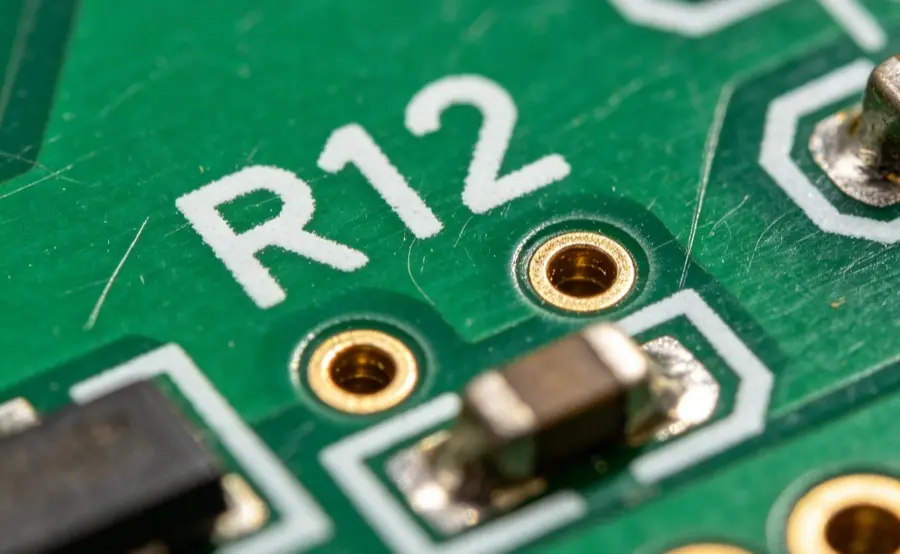
- Referenční označení (R1, C12, U3)
- Obrysy součástí a orientační značky
- Polarita elektrolytů, diod a LED diod
- Indikátory pinů 1 pro integrované obvody
- Štítky konektorů
- Zkušební body (TP1, TP2)
- Výstrahy a symboly vysokého napětí
- Loga, QR kódy, revizní text
Inkousty jsou obvykle na bázi epoxidu nebo vytvrzují UV zářením. Epoxidové barvy mají obvykle silnou přilnavost a dobře odolávají pájecímu teplu. Inkousty vytvrzované UV zářením rychle schnou a jsou vhodné pro velké objemy.
Záleží také na podkladu a povrchové úpravě. FR4 je obvyklý a tiskne se z něj pěkně. Materiály Rogers někdy vyžadují specifické složení inkoustu. Flex PCB jsou složitější, protože povrch se pohybuje a inkoust se musí také ohýbat. A povrchové úpravy jako HASL mohou vytvářet nerovnoměrnou topografii, která znesnadňuje jemný sítotisk, zatímco ENIG je rovnější a přívětivější.
Dvě velké metody tisku (a proč by vás to mělo zajímat)
Většina sítotiskových legend, se kterými se setkáte, je vyrobena pomocí jedné z nich:
Liquid Photo Imaging (LPI)
LPI používá světlocitlivý inkoust a proces expozice. Je běžný v sériové výrobě a bývá trvanlivý. Dokáže udržet slušné detaily, ale jako u každého procesu i zde platí pravidla pro minimální řádky a text.
Přímý tisk legendy (DLP)
DLP je v podstatě přímý tisk, často inkoustový, přímo na desku plošných spojů. Vynechává fólie a vyvolávací kroky, může být rychlejší a dokáže vytvářet detailní legendy. Často se také popisuje jako o něco méně odolný než LPI, v závislosti na systému inkoustu a vytvrzování.
Praktický závěr pro designéry je jednoduchý.
I když prodejce dokáže vytisknout velmi jemné prvky, vaše výnos klesne, když přitlačíte sítotisk k okraji. A čitelnost klesá ještě dříve. Proto se snažíme o “spolehlivé výtisky”, nikoliv o “výtisky v laboratorní ukázce”.
Nejlepší styl písma pro sítotisk PCB
Chcete písmo, které zůstane čitelné, když:
- tah se mírně zhušťuje rozetřením inkoustu.
- tisk se trochu posune od tolerance registrace.
- deska je pod úhlem při osvětlení na stole.
- zbytky tavidla a prach existují (protože vždy existují).
Používejte jednoduchá, standardní bezpatková písma.
Praktické možnosti:
- jednobarevná / vektorová písma (často se používají ve výchozím nastavení nástrojů CAD).
- Jednoduchá bezpatková písma podobná Arial, Helvetica, DIN style
- Vestavěná písma PCB CAD “Default” nebo “Proportional”, pokud je známo, že se vykreslují čistě.
Proč ne efektní písma?
Protože serify a kontrasty tenkých a silných tahů se na sítotisku rychle oškliví. Kudrlinky se vyplní. Drobné mezery se uzavřou. Písmena “R” a “P” začnou vypadat jako stejné písmeno. Není to designový plakát, je to návod k použití na továrním objektu.
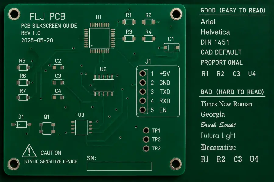
Vyhněte se těmto typům písma
- Velmi tenké tahy
- Vysoce kontrastní tahy (silné svislice, tenké vodorovné tahy)
- Dekorativní prvky
- Kurzíva v malých velikostech
- Všechna velká písmena v malém textu (velká písmena snižují tvarovou rozmanitost, paradoxně se hůře čtou, když jsou malá)
Ještě jeden nudný, ale důležitý bod
Udržujte konzistenci. Stejný styl písma na celé tabuli. Pokud styly mícháte, vypadá to nepřehledně a znesnadňuje to skenování při sestavování.
Nejlepší velikost textu pro sítotisk na PCB (co skutečně funguje)
Mnoho lidí uvádí “minimální velikost textu 1,0 mm”. Je to slušné pravidlo, ale je třeba ho rozvést. Velikost textu neznamená téměř nic bez šířky tahu.
U sítotisku na desky plošných spojů je nejdůležitější:
- výška znaku
- šířka tahu
- rozestupy mezi tahy
- a zda bude text oříznut otvory v pájecí masce, podložkami nebo dvorními zábranami.
Zde jsou uvedena praktická, výrobně bezpečná doporučení, která obvykle přežijí běžné výrobní tolerance.
Doporučené velikosti textu pro sítotisk (obecně)
Pro referenční označení a štítky, které mají lidé přečíst bez mikroskopu:
- Výška postavy: 1,0 mm až 1,5 mm přednostně
- Minimální výška znaku: 0,8 mm (pouze pokud opravdu musíte)
- Šířka tahu: Přednostně 0,15 mm až 0,20 mm
- Minimální šířka tahu: 0,12 mm (opět pouze v případě nutnosti)
Pokud označujete husté oblasti a smíříte se s tím, že to může být “sestava čitelná se zvětšením”:
- Výška postavy: 0,8 mm až 1,0 mm
- Šířka tahu: 0,12 mm až 0,15 mm
Pokud potřebujete text “viditelný zpoza stolu” (názvy konektorů, upozornění na polaritu):
- Výška postavy: 1,5 mm až 2,5 mm
- Šířka tahu: 0,18 mm až 0,25 mm
Tyto rozsahy nejsou magické zákony. Jsou to hodnoty “pravděpodobně toho později nebudete litovat”.
Důležité jsou mezery mezi písmeny
Například otvor uvnitř písmene “O” nebo “P”. Pokud je příliš malý, vyplní se a vzniknou kapky. Takže i když je šířka vašeho tahu technicky tisknutelná, geometrie písma taková být nemusí.
Proto vítězí jednoduchá písma. Udržují čítače otevřené.
Nejlepší šířka čáry pro sítotiskové obrysy a symboly
Sítotisk není jen text. Jsou to obrysy, tečky na vývodu 1, značky polarity plus, šipky, trojúhelníkové indikátory, kolečka testovacích bodů.
Doporučené šířky čar:
- Obecné obrysy a symboly: 0,15 mm až 0,20 mm
- Minimální (pokud to vaše fab umožňuje): 0,12 mm
- Výraznější varování nebo značky polarity: 0,20 mm až 0,30 mm
Při příliš tenkém tisku se linky lámou nebo blednou. Pokud jsou příliš tlusté, ztrácejí přesnost a mohou se srazit s jinými prvky.
Vyplněné tvary vs. obrysy
Vyplněné tvary (plné trojúhelníky, plné kruhy) jsou při tisku šetrnější. Pokud potřebujete indikátor pin 1, který se vždy zobrazí, je vyplněná tečka často lepší než malé obrysové kolečko.
Pravidla pro uvolnění: kam se sítotisk NESMÍ umístit
Většina továren automaticky ořízne sítotisk, který překrývá otvory pro pájecí masku, podložky a obnaženou měď. To je dobře. Ale také to znamená, že váš text může být rozsekán na nesmysly.
Proto je třeba při návrhu myslet na volný prostor a nespoléhat se na automatické ořezávání.
Praktické odstupy:
- Sítotisk na pájecí plošky: nejméně 0,15 mm, nejlépe 0,20 mm.
- Sítotisk do otvorů: nejméně 0,15 mm až 0,20 mm
- Sítotisk na okraji desek: alespoň 0,25 mm (více, pokud bude hrana frézována hrubě).
- Sítotisk na tělo součásti: nechte si prostor, aby byl štítek viditelný i po montáži.
Vyvarujte se také umísťování sítotisku přes přehrady pájecí masky mezi podložkami. I když se vytiskne, může vypadat rozmazaně a špinavě.
Maskované vs. nemaskované průchodky
Pokud jsou průchodky stanové (zakryté pájecí maskou), lze po nich bezpečněji přejíždět sítotiskem. Pokud jsou průchodky otevřené, může se barva rozšířit do otvorů nebo se kolem otvoru přetrhnout. U hustých vzorů často zlepšuje kvalitu tisku stanování průchodek pod sítotiskem.
Výběr barev: co je skutečně čitelné
Standardní barvy sítotisku: bílá, černá, žlutá. Nejlepší volba závisí na barva pájecí masky a zobrazovací prostředí.
Běžné párování:
- Zelená pájecí maska: bílý sítotisk je výchozím nastavením z nějakého důvodu.
- Černá pájecí maska: bílý sítotisk funguje, žlutý může také pop
- Bílá pájecí maska: černý sítotisk je obvykle tah
- Červená/modrá pájecí maska: bílá obecně funguje, ale kontrast se může lišit podle povrchové úpravy.
Lidé zapomínají na jednu věc. Povrchová úprava mění odrazivost. ENIG je lesklý, HASL může být místy nerovnoměrný a odrazivý. Při jasném světle jsou některé nápisy hůře čitelné, i když je kontrast “teoreticky” v pořádku.
Pokud vám záleží na čitelnosti, nevybírejte nízký kontrast kvůli estetice.
Tipy pro umístění, které vám později ušetří
Několik návyků, které zvyšují rychlost montáže a snižují počet chyb.
Umístěte referenční označení na viditelné místo po montáži.
Zní to samozřejmě. Ne vždy se to dělá.
- Pokud je to možné, umístěte odpadky mimo nádvoří komponenty.
- V případě integrovaných obvodů umístěte refdes poblíž pinů 1, ale ne pod čip.
- U pasivů umístěte refdes důsledně zarovnané, stejný směr čtení v celé desce.
Značky orientace a polarity by měly být nadbytečné.
Pro diody, LED diody, elektrolytické prvky. Použijte obojí:
- symbol polarity na sítotisku
- a zřetelnou grafiku otisku (např. výřez, sloupec, znaménko plus).
- a v ideálním případě konzistentní knihovní standard
Protože pokud se jeden z nich odstřihne, druhý často přežije.
Označte testovací body, jako byste to mysleli vážně
Pokud bude deska zkoušena:
- Označení zkušebních bodů “TPxx”
- Pokud to místo dovoluje, uveďte název sítě nebo napětí (TP5 3V3).
- Použijte dostatečně velký kruh nebo cílový symbol, abyste jej rychle našli.
Štítky s testovacími body neumisťujte na místa, která budou zakryta stíněním, chladiči nebo vysokými konektory.
Jak si výrobní reality pohrávají se sítotiskem (a jak ho obejít)
Sítotisk může selhat několika předvídatelnými způsoby.
Nesouosost a posun registrace
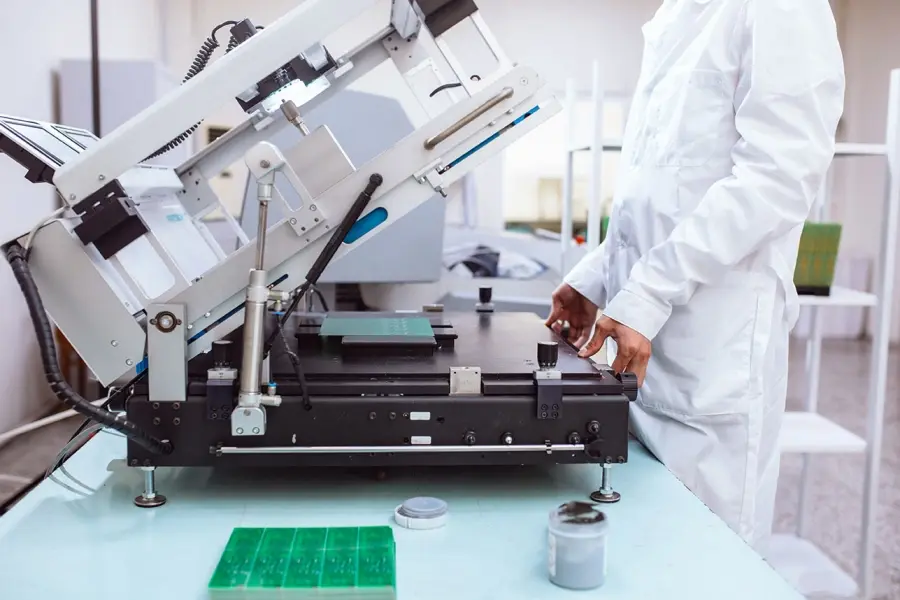
Mezi příčiny patří chyby při registraci, deformace desky a procesní tolerance. Při ručním sítotisku je zarovnání více závislé na obsluze. Automatizované tiskárny mohou dosáhnout mikrometrického zarovnání, ale nic není dokonalé.
Navrhněte kolem něj:
- neumísťovat text příliš blízko podložek
- vyhnout se drobným prvkům, které jsou závislé na dokonalém zarovnání.
- dává symbolům malou rezervu navíc
Rozmazávání a roztírání inkoustu
Často kvůli nadměrnému množství inkoustu, nesprávné viskozitě, znečištění nebo nesprávnému vytvrzení.
Továrnu nemůžete ovlivnit viskozita inkoustu z CADu, ale můžete:
- vyhnout se velmi tenkým tahům
- vyhnout se nacpávání textu mezi bloky
- používat jednodušší tvary písmen
Chybějící nebo vybledlé otisky
Opotřebovaná síta, špatná přilnavost, působení prostředí, špatné cykly vytvrzování. Opět jde o problémy na straně výroby, ale váš návrh pomáhá tím, že se drží v rámci pohodlných velikostí prvků.
A na skladování záleží. Vlhkost a výkyvy teplot mohou ovlivnit kvalitu. Pokud jsou desky určeny do náročných podmínek, poraďte se s výrobcem o typu inkoustu a očekávané trvanlivosti.
IPC a konvence symbolů (rozumný přístup)
Uvidíte odkazy na normy, jako je IPC-7351, pro vzory pozemků a pokyny pro umístění. Existují také normy týkající se konvencí značení, kontroly, trvanlivosti a obecné přijatelnosti výroby.
V praxi se při navrhování sítotisku uplatňuje “myšlení IPC”:
- Používejte jasné a konvenční symboly.
- Zachovejte čitelnost textu.
- Neumisťujte značky na místa, kde by překážely pájení nebo kontrole.
- Sestavení je jednoznačné.
Pokud se zabýváte zdravotnictvím, automobilovým a leteckým průmyslem, pak ano, měli byste se přizpůsobit přesným standardním požadavkům na značení a sledovatelnost. Pro většinu komerčních desek je stále výhodné dodržovat stejnou disciplínu.
Speciální případy: flexibilní desky plošných spojů a desky s vysokou hustotou.
Flexibilní desky plošných spojů
Flex desky se ohýbají. Inkoust se také musí ohýbat a přilnavost může být obtížnější. Tiskový tlak a napětí síta jsou citlivější, takže velmi jemné legendy jsou rizikovější.
Pokud je vaše flexi konstrukce hustá, zvažte:
- zachování minimálního množství sítotisku
- použití větších a výraznějších značek
- alternativní metody značení, jako je inkoustový tisk nebo laserové značení (trvalejší, často přesnější).
Desky s vysokou hustotou
Někdy prostě není místo.
Co funguje lépe než zmenšování všeho:
- Přesuňte některá označení na výkres sestavy místo na desku.
- Používejte méně, ale smysluplnějších označení (pouze konektory, polarita, klíčové IC).
- Pro revizi a sledovatelnost používejte QR kódy nebo 2D kódy, pokud to vaše továrna podporuje, ale čitelnost otestujte na skutečných vzorcích.
Rychlý kontrolní seznam: moje “bezpečná výchozí” pravidla pro sítotisk
Pokud chcete začít, můžete se přihlásit do většiny komisí:
- Jednoduché bezpatkové písmo, konzistentní ve všech oblastech
- Výška textu 1,0 mm až 1,5 mm pro refdes, kde je to možné
- Šířka tahu 0,15 mm až 0,20 mm
- Šířka čáry sítotisku 0,15 mm až 0,20 mm
- Vůle k podložkám a obnažené mědi Přednostně 0,20 mm
- Nespoléhejte na automatické ořezávání, umístěte legendy tak, aby přežily.
- Označení polarity a kolíku 1 je zřejmé a nadbytečné.
- Zvolte barvu sítotisku pro kontrast, ne pro vibrace
Není to okouzlující. Ale dobře se tiskne a dobře se čte.
Poznámka k sítotiskovým službám a výrobě
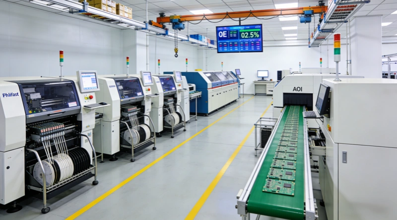
Mnoho výrobců desek plošných spojů zahrnuje sítotisk jako standardní možnost, včetně služeb jako PCBGOGO a mnoha dalších. Ať už je vaše deska vyrobena pomocí LPI nebo DLP, výše uvedené základy návrhu stále platí.
Pokud tisknete ručně ve vlastní režii, počítejte s větší variabilitou a většími problémy se zarovnáním. Automatizované sítotiskové tiskárny jsou rychlejší a konzistentnější pro sériovou práci, ale váš návrh musí být stále vyrobitelný.
A ano, pokud jste někdy viděli desku, kde jsou legendy mírně posunuté a chybí polovina označení “R”, obvykle to není proto, že by designér “zapomněl”. Je to proto, že návrh seděl na samé hranici možností procesu.
Získejte svou nabídku PCB ještě dnes
Hledáte spolehlivého partnera pro sítotisk a výrobu kompletních desek plošných spojů? Philifast je zde, aby podpořil váš projekt od návrhu až po dodání. Kontaktujte nás a získejte rychlou a profesionální nabídku.
Často kladené otázky (FAQ)
Co je to sítotisk na desce plošných spojů a proč je důležitý?
Sítotisk na desce plošných spojů je nevodivá vrstva inkoustu natištěná na desce, která označuje součástky, vývody 1, polaritu, konektory, propojky, testovací body, varování, loga a revizní kódy. Poskytuje veškeré informace zaměřené na člověka, které pomáhají montážním technikům správně umístit součástky, pomáhají zkušebním technikům rychle lokalizovat body a pomáhají při budoucí údržbě nebo řešení problémů.
Jaké materiály a barvy se běžně používají pro sítotisk na desky plošných spojů?
Při sítotisku na desky plošných spojů se obvykle používají nevodivé barvy na bázi epoxidů nebo UV záření. Mezi běžné barvy patří bílá, černá a žlutá. Epoxidové inkousty mají silnou přilnavost a dobře odolávají pájecímu teplu, zatímco inkousty vytvrzované UV zářením rychle schnou a jsou vhodné pro velkosériovou výrobu.
Jaké jsou hlavní metody tisku sítotisku na desky plošných spojů a jak se liší?
Dvěma hlavními metodami tisku jsou Liquid Photo Imaging (LPI) a Direct Legend Printing (DLP). Technologie LPI používá světlocitlivý inkoust s expozičním procesem běžným v sériové výrobě a bývá trvanlivá. DLP zahrnuje přímý inkoustový tisk na desku plošných spojů, který umožňuje rychlejší zpracování a jemnější detaily, ale může být o něco méně odolný v závislosti na použitém systému inkoustu.
Jaké styly písma se doporučují pro sítotisk na desky plošných spojů, aby byla zajištěna čitelnost?
Doporučují se jednoduchá, standardní bezpatková písma, jako jsou písma s jedním tahem/vektorová písma nebo písma podobná stylům Arial, Helvetica nebo DIN. Vyhněte se písmu se serify, tenkými tahy, ozdobnými prvky, kurzívou v malých velikostech nebo všemi velkými písmeny v drobném textu. Jednotnost stylu písma v celém textu zlepšuje čitelnost při montáži.
Jaké jsou nejlepší zásady velikosti textu pro sítotisk na desky plošných spojů, aby byla zajištěna čitelnost po výrobě?
U referenčních označení a štítků určených pro čtení člověkem bez zvětšení: výška znaku by měla být v rozmezí 1,0 až 1,5 mm (v případě potřeby minimálně 0,8 mm) a šířka tahu by měla být v rozmezí 0,15 až 0,20 mm (v případě potřeby minimálně 0,12 mm). Přiměřené rozestupy mezi tahy jsou rovněž zásadní pro zachování zřetelnosti i přes rozprostření inkoustu nebo posuny registrace během výroby.
Lze sítotisk použít jako náhradu pájecí masky na deskách plošných spojů?
Ne, sítotisk není náhradou pájecí masky. Pájecí maska zabraňuje vzniku pájecích můstků a chrání měděné stopy; sítotisk slouží výhradně jako označovací vrstva pro komunikační účely, jako je označování součástek a testovacích bodů. Použití sítotisku k opravě rizik spojených s pájením může vést k problémům, jako je vypálení nebo rozmazání inkoustu.