
PCB Prototype Manufacturing for Your Next Design Revision
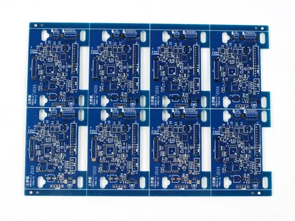
Make your next design a physical board you can evaluate. FLJ PCB / Philifast in Shenzhen supports custom bare-board prototypes with engineering review, material selection and electrical testing—then helps you plan the next revision.
Build the sample around what you need to learn
A PCB prototype is an early build of your custom printed circuit board. It gives your team a physical design revision to check before committing to a larger order. Start with the question the sample needs to answer; we can help connect that goal with the fabrication choices.
Check fit and connections
Evaluate the outline, mounting holes, connector openings and copper layout. A bare board can support a mechanical fit check; circuit bring-up follows after components are fitted.
Evaluate a demanding construction
For high-speed, RF, power or flexible circuits, choose the material, copper, stackup and mechanical features that matter to the experiment. Explain the operating conditions you want to investigate.
Prepare for a repeatable build
Use the prototype to resolve engineering questions and capture changes. A reviewed revision becomes a better starting point for a pilot run and subsequent production.
Prototype PCB options for your design
Your prototype does not have to be a basic two-layer board. We review the construction your circuit needs, including dense interconnects, controlled impedance and specialist materials.
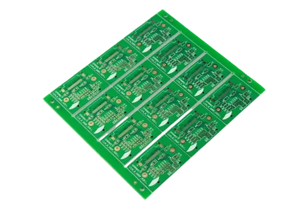
Rigid & multilayer prototypes
FR4 PCB prototypes for control boards, sensors and general electronics, including 2-layer, 4-layer and more complex stackups.
Explore this construction ↗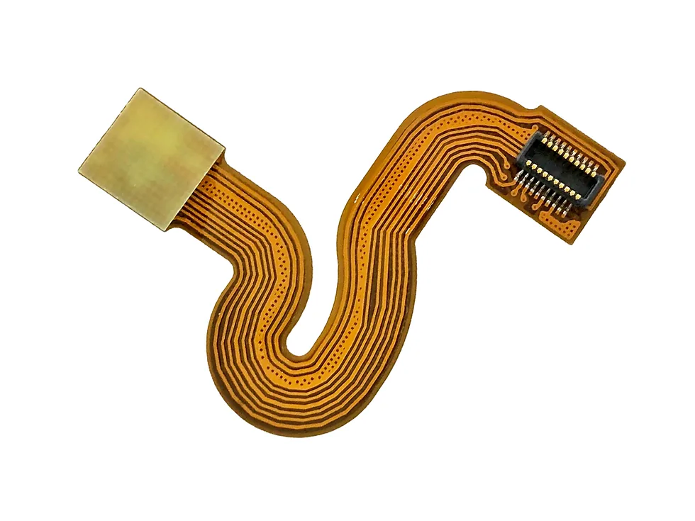
Flex & rigid-flex prototypes
Explore connector fit, mounting regions and the intended flex path. Review bend locations, coverlay and stiffeners with the mechanical design.
Explore this construction ↗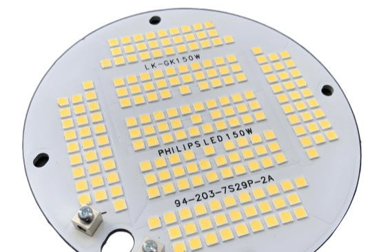
Metal-core prototypes
For LED and power designs, connect the insulated circuit layer with the proposed thermal path, mounting and heat-sink arrangement.
Explore this construction ↗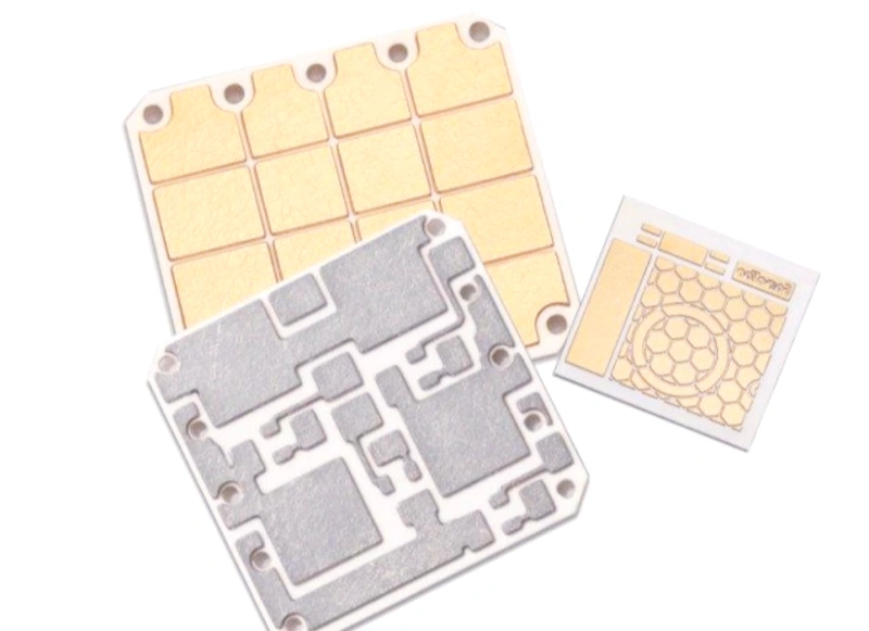
Ceramic prototypes
Discuss a specialist substrate when electrical insulation, temperature or heat transfer shapes the design. Metallization and mounting are part of the review.
Explore this construction ↗Prototype fabrication capabilities
These references come from FLJ’s published manufacturing capabilities. Our team reviews how the features work together for your board; the selected prototype specification is confirmed in the quotation.
| ویژگی | Published manufacturing scope | Prototype planning |
|---|---|---|
| General rigid-board layers | 1–30 layers | Choose around routing, planes and the stackup you want to validate. |
| Line / space at 0.5 oz copper | 3 / 3 mil | A copper-specific reference; heavier copper needs different geometry. |
| Finished copper, general scope | Outer up to 8 oz; inner up to 6 oz | Review copper weight with clearances and the thermal/current requirement. |
| Finished mechanical holes | 0.10–6.2 mm | Hole depth, material and plating affect the applicable range. |
| Controlled impedance tolerance | ±5 Ω below 50 Ω; ±10% at or above 50 Ω | Confirm the target, stackup and verification for the quoted build. |
| گزینههای پرداخت سطح | ENIG, lead-free HASL, OSP, immersion tin/silver, plated gold | Select for soldering, contacts and the intended evaluation. |
Keep the material and stackup relevant to your test
For an early fit check, a simpler construction may answer the immediate question. For signal integrity, thermal behavior or production validation, a representative material and stackup usually give more useful results.
Tell us if the prototype needs the intended production laminate. We can discuss FR4, high-Tg FR4, RF laminates, polyimide and metal-based systems around the application, availability and schedule. Any proposed alternative is discussed with your team.
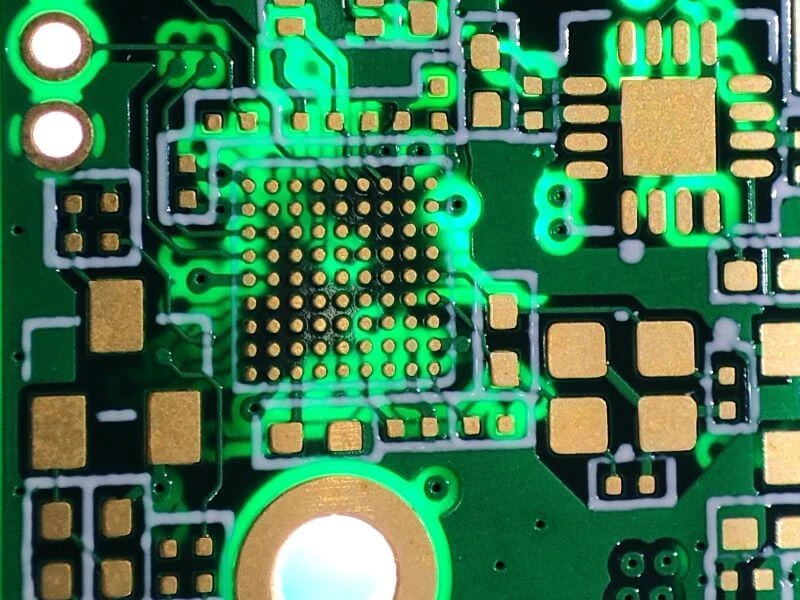
For controlled impedance prototypes, review the dielectric spacing, reference planes, finished copper and trace geometry together. The final pressed dielectric thickness matters to the calculation. Keeping these choices recorded helps your team compare the prototype with the next build.
Engineering feedback before your first board is made
Send the current design and tell us what is still open. We review the fabrication data, raise specific questions and work with you on practical choices before releasing the board for manufacture.
Copper, holes and pads
Review spacing, annular rings, plated holes and non-plated openings with the selected copper and board depth.
Outline and handling
Check slots, cutouts, connector fit and whether individual boards or an assembly panel suit your next step.
Stackup and special features
Connect layer order, via structure, impedance and filling requirements with a workable process route.
One agreed design revision
Confirm any proposed manufacturing change with your team and keep the released files connected to the order.
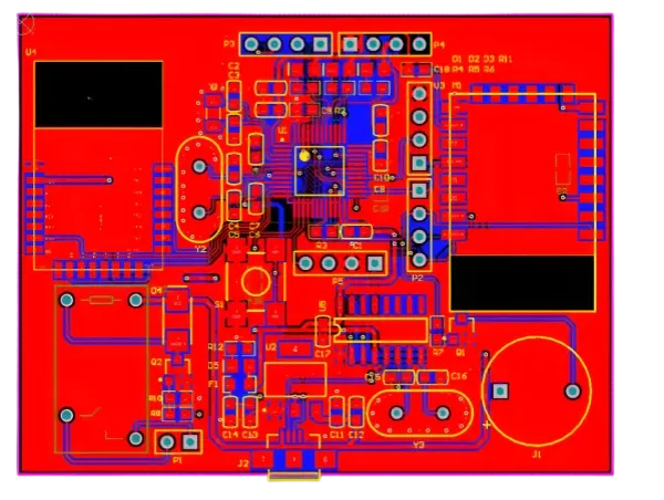
Your CAD design-rule check and our fabrication review serve different purposes. A manufacturing review helps identify process issues; circuit performance is evaluated through your assembled prototype and test plan.
How your prototype takes shape
The engineering review gives the build a clear starting point. We then follow the agreed board construction and keep the sample connected to its released design revision.
- 01
Share the design
Send available board files, the sample quantity and the target date if known.
- 02
Review together
Resolve useful engineering questions and agree the prototype construction.
- 03
Fabricate the boards
Build the released revision through the process appropriate to its stackup.
- 04
Inspect and test
Check workmanship, dimensions and agreed bare-board electrical requirements.
- 05
Deliver and evaluate
Receive protected boards for assembly, fit checks and your design evaluation.
Know what the prototype has been checked for
Bare-board electrical testing checks intended connectivity and isolation. Physical and visual checks address features such as holes, outline, solder mask, markings and finished surfaces. We can discuss the inspection and reporting appropriate to your prototype.
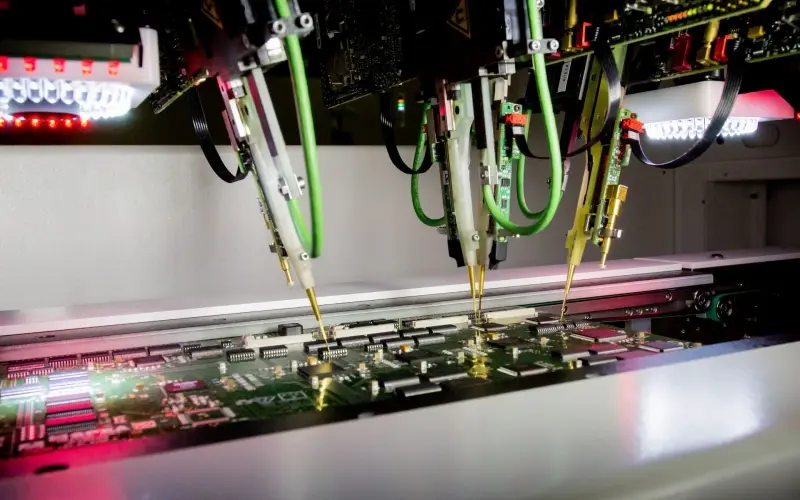
Flying-probe testing is useful for many sample builds because it can test without a dedicated bed-of-nails fixture. The test approach is selected around the board, quantity and agreed coverage. Controlled impedance measurements and other specialist checks are addressed with their targets and method.
A passed bare-board test does not establish that the finished product functions correctly. Power-up, firmware, signal integrity and application performance are evaluated after assembly. Share any supplier-qualification or acceptance needs so we can connect them with the relevant inspection records.
Need components fitted to your prototype?
Prototype PCB fabrication supplies the bare board. Prototype PCB assembly adds components and soldering so your team can bring up the circuit and run functional checks. FLJ also supports the assembly route when you need populated engineering samples.
Send the PCB design with your available BOM, placement information or assembly notes. We can discuss component sourcing, customer-supplied parts, mixed SMT/through-hole work and the inspection or test support your sample needs. A BOM is useful for assembly; it is not needed to manufacture a bare board.
A prototype is one step in your design iteration
Keep the fabrication revision beside your evaluation notes. That makes it easier to distinguish a design change from a manufacturing or material change when comparing results.
Capture what you learned
Record fit, connector access and test findings with the board revision. Photos and marked-up drawings help explain what you want to change.
Review the next build
Send updated files or a change list. We can review the effect on stackup, holes, copper, panelization and the manufacturing route.
Move toward a pilot run
Once the design is ready, discuss a small production build. Confirm the released specification and any changes in inspection, packaging or quantities.
Plan prototype cost and turnaround together
A useful prototype quote connects the board specification with your evaluation plan. Tell us the number of boards you need and the date you are working toward; we can review the manufacturing options with you.
Board construction
Layer count, board area, copper, via structures and special machining affect fabrication effort.
Materials and finish
A nominated laminate or specialist finish can affect availability. Discuss alternatives if the experiment allows them.
Sample quantity
Include boards for bring-up, separate test teams, destructive evaluation or a spare when planning the quantity.
Schedule and delivery
Build timing depends on engineering review, material and process route. Shipping is planned separately from fabrication.
If the date is the main priority, ask about quick-turn PCB fabrication. We will review what is feasible for the actual design and confirm the build and shipping plan in the quote.
Send the design you have
Gerber artwork and drill data are a helpful starting point. A board drawing, stackup or fabrication notes can explain the details that matter to your sample. If you currently have a native CAD file or an incomplete package, send it and describe the project—we will follow up on what is needed.
PCB prototype FAQs
How much does a PCB prototype cost?
The quote depends on board area, quantity, layers, material, copper, vias, finish and test scope. Send the current design for a project-specific quote. If some choices remain open, explain what the prototype needs to demonstrate so we can discuss suitable options.
How long does prototype PCB fabrication take?
Timing depends on the reviewed design, material availability, process route and requested quantity. Share your target date and we will confirm a feasible manufacturing schedule. Shipping time is separate; date-sensitive projects can be reviewed for a quick-turn route.
Can I send PCB files before every detail is decided?
Yes. Send the current files and explain what is still undecided. Gerber and drill data are useful, but our team can discuss your available CAD files, drawings and notes, then follow up on the details needed for the build.
What quantity should I order for a prototype?
Plan around your evaluation: bring-up, fit checks, separate test teams, spare boards and any destructive tests. Tell us the requested quantity and we will review the practical fabrication and delivery options rather than assume one sample count fits every project.
Should a prototype use the final production material?
Use a representative material and stackup when electrical, thermal or mechanical behavior is the purpose of the test. A simpler board can be useful for an early fit check, provided your team understands which results it can demonstrate.
Does a PCB prototype receive a functional test?
A bare-board electrical test checks connectivity and isolation, not circuit function. Functional evaluation requires an assembled board and a defined test plan. If you need populated samples, discuss prototype PCB assembly and the required inspection or test support.
Can you make multilayer, HDI and flexible PCB prototypes?
We review multilayer, HDI, flex, rigid-flex and specialist prototype constructions with the design. The applicable layer stack, materials, holes, geometry and test scope are confirmed together for the quoted board.
Can an approved prototype be ordered again for production?
An approved prototype is a useful starting point. Before the next order, confirm the design revision and review changes in materials, stackup, panelization, quantity and inspection. Updated design files identify a new revision for review.
From a design revision to a board you can evaluate
Send your available PCB files or project questions. Our team will help you work through the next step.