Selecting a contract electronics manufacturer is one of the most important decisions in product development. Over our 15 years of operating SMT lines and building complex assemblies, we have seen great designs fail because of poor supplier choices — and simple designs succeed through the right partnership.
This guide gives you a practical, engineer‑to‑engineer checklist. We will walk through the real pcba manufacturer selection criteria that matter on the factory floor. You will learn how to evaluate pcb assembly quality standards, compare pcba testing methods (aoi, x-ray, flying probe), break down pcba cost factors, and understand the trade‑off between pcba turnkey vs consignment. We also cover the crucial difference between ipc‑a‑610 class 2 vs class 3, how to use a pcba dfm checklist, what rapid prototyping pcb assembly really means, and how to read a pcba lead time breakdown. By the end, you will have the same pcba supplier audit checklist we use internally — and the insight to evaluate pcba quotation evaluation و pcba moq requirements like a seasoned buyer.
Let’s get started, no fluff, just factory‑proven facts.
Ready to Start Your PCBA Project?
Philifast offers fast-turn PCB assembly, DFM review, and reliable manufacturing backed by 15+ years of experience.
1. Manufacturer Experience and Technical Expertise
A company’s track record in producing designs similar to yours is the strongest predictor of success. Look for specific experience with your PCB technology — single‑sided, double‑sided, چندلایه, rigid‑flex — and your type of components, from 01005 passives to large BGAs.
Ask these questions early:
- How many years has the factory done PCBA? (15 years of consistent SMT and through‑hole production is a solid baseline.)
- Can they share examples of boards with the same layer count, copper weight, and surface finish you use?
- Do they have in‑house engineering staff who give DFM feedback before the first run?
A manufacturer that only does simple consumer boards may struggle with a 12‑layer high‑density design for an aerospace application. Pcba manufacturer selection criteria start with this match: your complexity and their proven capability must align. No amount of marketing claims can replace a factory visit or a detailed audit of their process records.
2. Quality Standards: Beyond the Certifications
Every competitor article tells you to look for ISO 9001 and mention IPC‑A‑610. Certifications are important, but they only show a factory has a documented system — not how well it is executed. In our facility, we build to IPC‑A‑610 Class 2 and Class 3 daily, and the difference defines your cost and reliability.
Class 2 vs Class 3 – Choosing the Right Acceptance Level
IPC‑A‑610 defines three classes of electronic assembly acceptance. Class 1 is for general consumer products, Class 2 for dedicated‑service products, and Class 3 for high‑reliability where failure cannot be tolerated. The key decision is between Class 2 and Class 3, which we often explain to customers.
- Class 2 allows a moderate level of imperfections. For example, solder joint fillet height can be slightly less than perfect, and voiding in BGAs up to 25% is accepted. It is sufficient for most industrial controls, consumer IoT, and automotive interior electronics.
- Class 3 demands tighter tolerances: voiding must be below 15%, solder volume is strictly defined, and lead protrusion in through‑hole parts has narrower limits. This adds about 20–30% more inspection time and cost because every joint must be verified to stricter criteria.
Why does this matter? We often see startups specifying Class 3 for a consumer gadget “just to be safe.” That decision alone can inflate the assembly cost by 25% without any real field reliability gain. Conversely, a medical device or satellite hardware must meet Class 3 — the added inspection is a fraction of the cost of a potential failure. Good pcb assembly quality standards advice is: choose the acceptance class your product truly needs, not the highest one by default. Our engineers always help you map the environmental and reliability requirements to the right class during the quotation phase.
Beyond IPC‑A‑610, a capable supplier will also follow J‑STD‑001 for soldering process requirements and maintain calibrated measurement systems. Ask if they do solder paste inspection (SPI) immediately after printing and before component placement — that single step catches about 70% of potential solder defects before they become rework.
3. Inspection and Testing Capabilities
Competitor articles list AOI and X‑ray as a checkbox. In reality, AOI alone cannot find every defect, and even 2D X‑ray misses the most dangerous BGA failures. A proper test strategy layers multiple methods.

Beyond AOI: The Test Strategies That Save Field Returns
We combine three stages of inspection to bring field DPPM (defects per million opportunities) to single‑digit levels:
- Inline AOI (100% of boards) – Inspects component presence, polarity, tombstoning, and solder bridging on all visible joints. It works at line speed and stops a misplaced 0201 from leaving the line.
- 3D X‑ray (sample or 100% for BGAs/QFNs) – 2D X‑ray shows solder shorts and large opens, but it cannot reliably detect “head‑in‑pillow,” where the BGA ball and solder paste touch without complete wetting. Head‑in‑pillow often causes intermittent opens that pass initial functional test and fail only after thermal cycling. Only 3D X‑ray or CT can reveal these hidden defects with confidence.
- Flying Probe Electrical Test – For prototypes and mid‑volume, the flying probe measures component values, tests nets for shorts/opens, and verifies diode and transistor orientation. It replaces a costly bed‑of‑nails fixture for many designs.
For high‑volume production, we may replace the flying probe with an In‑Circuit Test (ICT) fixture, which tests every net and component simultaneously. The key to choosing the right pcba testing methods (aoi, x‑ray, flying probe) is understanding which defects are most likely in your design. If you have dense FPGA or BGA packages, push for 3D X‑ray. If you have many analog circuits, flying probe can catch value errors. A manufacturer that only offers AOI and 2D X‑ray may leave critical failure modes unchecked.
We also strongly recommend a functional test at the end of the line, either designed by you or with our support, because electrical test alone cannot simulate real‑world operating conditions. A layered test approach reduces field returns by over 40% compared to AOI‑only inspection.
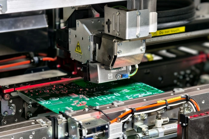
4. Technology and Equipment
Look past the generic “state‑of‑the‑art machinery” claims. Specific equipment determines what type of designs a factory can reliably run. A good evaluation covers these points:
- Placement speed and accuracy: What CPH (components per hour) can the line achieve? Can it handle 0201 (0.6 mm × 0.3 mm) or 01005 (0.4 mm × 0.2 mm) chips? Our YAMAHA and JUKI lines place down to 01005 and fine‑pitch BGAs with 0.3 mm ball pitch.
- Soldering capabilities: What reflow oven zones do they use? Can they do nitrogen atmosphere for improved solderability? Do they have selective wave soldering for mixed‑technology boards? In our factory, we combine dual‑lane reflow with selective wave and hand‑soldering stations for through‑hole components, which covers almost any design.
- Rework and repair: Boards will fail, even in the best process. Ask if they have hot air rework stations and follow IPC‑7711/7721 for rework procedures. A factory without good rework capability will scrap boards that could be saved.
Request actual photos of the factory floor, not just website stock images. If the equipment list names specific brands (YAMAHA, ASM, JUKI, Heller, Ersa), that shows transparency. If it only says “high‑speed SMT lines,” ask for details.
5. Design Support and DFM Feedback
A factory‑level DFM (Design for Manufacturability) review is one of the strongest differentiators between a simple assembler and a true manufacturing partner. A good supplier will look at your Gerber files and BOM before quoting, not after you pay for a prototype run that fails.
5 DFM Violations We See in 70% of New Designs
In our 15 years of doing DFM reviews, certain issues appear again and again. Here is a practical pcba dfm checklist from our engineering team:
- Missing copper thieving on outer layers – Large empty copper areas can warp the board during reflow, causing open joints. We add copper balancing (thieving) to keep the board flat, especially on thin laminates.
- Solder‑mask‑defined (SMD) vs non‑solder‑mask‑defined (NSMD) pad mistakes – For fine‑pitch BGAs, NSMD pads need at least 0.1 mm solder mask clearance; otherwise, tombstoning risk rises. We often adjust the mask opening when we see violations.
- Incorrect panelization – Tab‑routed panels with insufficient mouse‑bite holes leave fragile overhangs that break during depaneling. V‑score is fine for rectangular boards, but complex shapes need tabs. Our team redesigns the panel outline at no extra charge for proper handling.
- Test points not on a 0.1‑inch grid – A test fixture then costs two to three times more because it needs a custom‑drilled plate. We advise moving test points to standard grid to make ICT affordable.
- Silkscreen over pads – The ink contaminates the solder joint, leading to poor wetting and opens. We request a silkscreen clip around pads.
A manufacturer that provides this feedback at the quoting stage saves you at least one prototype iteration. That alone can cut your NPI cycle by two to three weeks. Insist on seeing a sample DFM report before you commit.
6. Prototyping and New Product Introduction (NPI)
Fast prototyping is not “only for long‑term partners.” A capable PCBA factory can turn around prototype quantities for new customers in a few days, provided the components are available. We have built thousands of prototypes with no MOQ and a standard lead time of 5 working days from kitted parts to shipment. But “rapid” only starts after all pre‑conditions are met.
What to Expect from a Quick‑Turn Prototype Run
Rapid prototyping pcb assembly means the assembly process itself is fast, but you must manage these pre‑steps:
- Gerber file approval (1–2 days if we find no major issues)
- Component kitting: If you supply parts, they must be at our dock complete. If we source turnkey, in‑stock parts arrive in 2‑5 business days, but special components can take 10 days or more.
- Stencil fabrication (same day or next day if ordered early)
So a realistic clock‑start‑to‑ship time is 8–12 working days for a 2‑ to 4‑layer board with standard components. Our factory offers a true 3‑day assembly service after parts are kitted for 2‑layer prototypes, and we can push to 24 hours for simple designs with a pre‑approved Gerber. Make sure your supplier explains what “rapid” means in days, not adjectives.
Also, confirm they support low‑volume PCB assembly (5, 10, 20 pieces) without a large NRE charge. For 5 pcs, the stencil cost ($80–150) is the main extra; we often waive programming fees for first‑time prototypes. If a supplier requires a long‑term commitment before building your first board, look elsewhere.
7. Production Capacity and Lead Time
Capacity is not just about how many SMT lines a factory has; it is about how they schedule work to meet your deadlines. A small factory with good planning can deliver faster than a large one with overloaded schedules.
The Anatomy of a PCBA Lead Time
When a supplier says “5‑day assembly lead time,” what does that really include? We break down a typical pcba lead time breakdown for a mid‑volume run:
- DFM review and Gerber approval – 1 to 2 working days (concurrent with purchasing if we spot no issues)
- Component procurement – 2 to 5 days for standard parts from authorized distributors; customs delays can add 2‑3 days for rare ICs
- Production scheduling – 0.5 to 2 days, depending on line availability
- Assembly (SMT + through‑hole) – 1 to 3 days for a few hundred boards
- Inspection and test – 1 to 2 days (includes AOI, X‑ray, flying probe, and optional functional test)
- Shipping – 1 to 3 days (air freight)
So a “5‑day” assembly promise is only for the production step itself. The total realistic timeline from file submission to dispatch is typically 10–15 working days. A transparent manufacturer will show you a Gantt chart‑like plan at the quotation stage. Demand that clarity.
For high‑volume orders, ask how many SMT lines the factory dedicates to your project and what the typical weekly throughput is. We can scale from 5 to 5000 boards per week by adding lines and shifts.
Ready to Start Your PCBA Project?
Philifast offers fast-turn PCB assembly, DFM review, and reliable manufacturing backed by 15+ years of experience.
8. Cost Factors and Pricing Models
Price matters, but the cheapest quote often hides risks: cheap component sourcing, no test, poor quality. A proper pcba quotation evaluation looks at the total cost, not just the per‑board assembly price. Pcba cost factors include:
- BOM cost – The largest slice. A manufacturer that sources from broker‑markets may give a lower component price but introduce counterfeit risk. Our turnkey purchasing uses only franchise distributors and we provide full traceability.
- Labor cost – Driven by the number of SMT placements, through‑hole parts, and any manual operations like conformal coating or potting. The assembly cost is often quoted per joint or per board.
- NRE (Non‑Recurring Engineering) – Stencil, programming, fixture, and any special tooling. Typical NRE for a prototype run is $200–400, regardless of quantity, so for 5 pieces that adds $40‑80 per board. For 1000 pieces, it is negligible.
- Test development – Functional test development adds to NRE but saves field returns.
Turnkey vs Consignment: A Total Cost Analysis
The choice between pcba turnkey vs consignment affects your cash flow and risk.
- Turnkey – The manufacturer buys all components, adds a 10–15% procurement fee (handling, sourcing, warranty). You receive one invoice and a fully built board. This saves you inventory management, but you pay the fee. For a $50 BOM on 500 units, turnkey cost is about $25,000 (BOM $22,500 + fee $2,500).
- Consignment – You supply all parts, no procurement fee. But you must hold 5–10% extra inventory for attrition and parts lost in the process. You also carry the risk of missing or counterfeit parts. On the same 500‑unit order, your direct BOM is $22,500, but you might need $3,000 extra inventory buffer and could face line‑down costs if one part is short. The net saving is often smaller than it appears.
Smaller companies or complex BOMs with long leadtime ICs benefit from turnkey because the manufacturer’s purchasing power can offset the fee. We offer both models and help customers run the numbers with a simple spreadsheet.
Finally, check pcba moq requirements. A good partner can start at 2–5 pieces without penalty, though NRE will be amortized over a small volume. We do not enforce an MOQ for SMT assembly, which is critical for hardware startups.
9. Material Sourcing and Surface Finishes
PCB base materials and surface finishes directly affect assembly yield, reliability, and cost. A manufacturer should explain your options clearly.
- Base laminates: Standard FR‑4 (Tg 130‑140°C) works for most consumer designs. High‑Tg 170‑180°C is needed for lead‑free soldering on thick, multilayer boards to prevent delamination. Rogers RO4350B or Isola materials are common for RF/microwave. We keep stock of standard FR‑4 and can order exotic materials within a week.
- Copper weight: 1 oz copper is standard; 2 oz is used for high‑current paths; 3 oz or higher requires special processing. We handle up to 3 oz inner layers and 2 oz outer routinely.
Surface finish is a common pcba surface finish comparison point because it affects solderability, shelflife, and flatness. Here is a quick reference:
- HASL (Lead‑free) – Low cost, good shelf life, but uneven surface — poor for fine‑pitch parts. We use it for simple, non‑flatness‑sensitive boards.
- ENIG (غوطهوری نیکل الکترولس با طلا) – Flat surface, excellent for fine‑pitch and BGA, moderate cost, shelf life >12 months. Our default for most prototypes.
- OSP (Organic Solderability Preservative) – Lowest cost, flat, but limited shelf life (6 months) and requires careful handling. Good for consumer products with quick assembly cycles.
- غوطهوری نقره – Good planarity, competitive cost, shelf life about 6–12 months, sensitive to handling and tarnish.
- حمام قلع – Flat, now less common, risk of whiskers.
Our engineers help you pick the right finish based on your design’s pitch, storage conditions, and budget. Poor finish choice is one of the preventable pcb assembly failure modes, especially when ENIG develops “black pad” defects. We control the plating process tightly to avoid those failures.
10. Communication and Customer Support
Daily project updates, a single point of contact, and fast issue resolution are not just nice‑to‑have — they prevent delays. In our factory, each customer gets a dedicated project engineer who provides:
- Real‑time online access to order status and inspection data
- Immediate feedback when a component becomes obsolete or out‑of‑stock, along with approved alternatives
- Video walkthroughs of first‑article builds for remote customers
Check how quickly the supplier responds to inquiry emails. Send a technical question on a Friday evening and note when you receive a response. A factory that operates across multiple shifts or has a customer portal will typically answer within a few hours. That responsiveness predicts how they will handle production crises.
11. Supplier Audit: A Practical Checklist
You do not need to visit every factory, but a structured pcba supplier audit checklist can be used remotely or on‑site. Use these points:
- Quality Management: Request copies of their ISO 9001 and IPC‑A‑610 certification certificates. Verify they are current.
- کنترل فرآیند: Ask for a sample PFMEA (Process Failure Mode and Effects Analysis) for a similar board. If they cannot produce one, process discipline is weak.
- Incoming Inspection: How do they verify components? Do they have a digital microscope and X‑ray for spot‑checking?
- Equipment Maintenance Records: Ask for the last calibration certificate for their SPI and AOI machines.
- قابلیت ردیابی: Can they trace a specific assembled board back to the reel of resistors and the date of placement? We use laser marking and barcode scanning for full traceability.
- Rework Documentation: Request their IPC‑7711/7721 rework procedure. Good rework prevents field failures.
- Environmental Compliance: Verify RoHS and REACH compliance. Ask for conflict minerals reporting if needed.
Use this checklist to score potential suppliers. A “no” on traceability or documented process control is a red flag.
سوالات متداول
How do I choose a PCB assembly company?
Start with a clear list of your technical requirements: board layers, component types, expected volume, and required quality class. Then use this article’s pcba manufacturer selection criteria to shortlist factories, check their DFM feedback, and evaluate their testing and communication. Always ask for a sample build before a full production order.
What certifications should a PCBA manufacturer have?
At a minimum, ISO 9001 for quality management. For assembly, compliance to IPC‑A‑610 and J‑STD‑001 is essential. If your product requires high reliability, ensure they can demonstrate Class 3 capability. Also, check for environmental certifications like ISO 14001 if that matters to your market.
How much does PCBA cost per board?
The cost depends on BOM, board complexity, volume, and services. For a typical 2‑layer board with 100 SMT placements in quantities of 100, you might pay $8–15 per board for assembly (excluding components). Prototype quantities (5 pcs) can be $30–50 each because NRE is spread over fewer units. Use a detailed quotation to understand the breakdown.
What is the difference between turnkey and consignment PCBA?
In turnkey, the manufacturer buys all parts and builds the board; you pay a single price that includes a component handling fee. In consignment, you supply all parts, no handling fee, but you manage inventory and risk. Turnkey simplifies the process, but consignment can save cost if you have a well‑managed supply chain.
How long does PCBA manufacturing take?
From final Gerber approval and all parts on‑hand, assembly can take 1–3 days. But the full cycle from file submission to shipment usually takes 10–15 working days due to DFM review, component procurement, and scheduling. Ask your manufacturer for a real lead time breakdown, not just assembly days.
What is a DFM check and why is it important?
A DFM (Design for Manufacturability) check reviews your PCB design files for issues that could cause assembly defects — pad size, solder mask clearance, panelization, etc. It prevents costly prototype failures and reduces the number of revision cycles. A good DFM report is free and provided before you commit to a build.
نتیجهگیری
Choosing the right PCBA manufacturer is not about finding the cheapest quote or the fanciest website. It is about identifying a partner that understands your technical needs, communicates transparently, and brings real manufacturing discipline. Use the pcba supplier audit checklist above, look for evidence of real DFM engagement, and demand specific test strategies, not just buzzwords.
Our factory has spent over 15 years helping engineers turn prototypes into reliable, volume‑produced electronics. We work to IPC‑A‑610 Class 2 and 3, combine inline AOI with 3D X‑ray and flying probe, and give detailed DFM feedback before any machine runs. If you are ready to move forward —
Contact us today to get a design review or a fast, transparent quotation. We are happy to walk you through our process and show you exactly how we build quality into every board.