
Double-Sided PCB Manufacturing
FLJ manufactures custom double-sided PCBs with copper circuits on both faces of the board and plated interconnections where the design needs them. We supply two-layer bare boards for prototypes and production, with the selected laminate, copper, holes and solderable finish. Component sourcing and assembly can continue the build when you need a populated board.
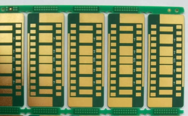
Two Copper Layers, One Connected Circuit
A double-sided PCB has a copper circuit on each side of an insulating core. It is also called a two-layer PCB: the layer count describes the conductive copper, rather than the solder mask, printed markings or number of faces populated with components.
The second copper face gives connections another route through the layout. A track can pass through a plated via to the opposite face, continue around a crowded area and reach another component or connector. For example, a connector signal can start on the top copper, pass through a via and continue on the bottom toward a control device. A separate top-side connection can cross that bottom route without touching it. This illustrates a routing choice rather than a measured customer design.
This extra routing space can support a smaller outline or a denser circuit. It does not require components to occupy both faces: a board with components on one face can still use both copper layers for its connections. The component layout and soldering route determine the assembly arrangement.
FLJ fabricates the two copper patterns, their plated connections and the finished board shape as one bare-board product. For simpler circuits, our single-sided PCB service provides a one-copper alternative; designs needing additional routing or reference layers can move to a multilayer construction.
Custom Two-Layer Board Configurations
The board construction connects the circuit with the product around it. FLJ supplies FR4 and high-Tg FR4 boards, with the selected laminate, finished copper, holes and surface finish carried into fabrication. Specialist material requirements are covered through our PCB materials and RF manufacturing services.
- Copper construction
- Two patterned copper faces with plated interconnectionsRouting between component and connector locations
- Laminate
- FR4 and high-Tg FR4 constructionsInsulation, support and assembly-temperature needs
- Finished thickness
- Thickness selected for the board drawing and constructionConnector, guide and enclosure fit
- Circuit copper
- Selected finished weight and conductor geometryCurrent paths, routing dimensions and etching conditions
- Solderable surfaces
- ENIG, lead-free HASL, OSP, immersion tin or silverExposed pads prepared for the soldering route
- Holes and profile
- Plated and non-plated holes, routed slots and finished outlineElectrical connections, lead fit and mounting
- Delivery form
- Individual boards or a production panelHandling, placement and board separation
What a Two-Layer Stackup Contains
The basic stack has top copper, an insulating core and bottom copper. The two conductor layers are part of the finished board thickness, but copper weight and overall board thickness describe different features. A material grade alone does not set either dimension.
Both outer faces share the work of signal routing, power and ground distribution. A continuous ground area can provide a useful return path, but a copper pour interrupted by routing is not equivalent to an uninterrupted reference plane. When the circuit needs more routing room and dedicated internal planes, a four-layer board may be the more suitable construction.
Copper, Mask and the Finished Surface
The starting copper foil and the copper deposited during fabrication contribute to the finished conductor. Finished copper weight therefore describes the produced circuit, not just the incoming laminate foil. Its thickness affects the relationship between trace width, spacing and the etched result. Solder mask then protects the intended copper areas and exposes the pads needed for assembly. Surface finishing treats the exposed copper; it is separate from the solder mask and from the copper that connects the layers through a hole.
FLJ’s manufacturing capabilities, material and surface-finish pages provide the wider specifications. This page focuses on the two-layer construction rather than combining every general manufacturing minimum and maximum into one board.
Plated Holes, Pads and Copper Continuity
Three Hole Roles
A via connects copper features on the two faces. A plated component hole also accepts a lead, making its finished opening part of the component fit. A mechanical mounting hole or slot performs a different job and can remain non-plated when no conductive connection is needed. A mounting feature intended for grounding can instead use a specified plated construction.
A conventional plated-through hole has copper on its wall and an open center. Plating the wall is different from filling the hole. Filled and capped via structures serve other design and assembly needs, covered on their dedicated fabrication pages.
From Insulating Hole Wall to Copper Connection
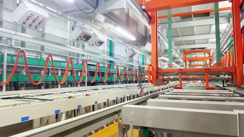
Drilling exposes the laminate along the hole wall. Cleaning and preparation establish a surface suitable for the conductive preparation and subsequent copper deposition. In a conventional electroless-copper route, a thin copper layer establishes the conductive foundation; later electroplating builds the copper connection. Suitable direct-metallization routes provide a different conductive preparation before the copper is plated.
Imaging, plating and etching form the required copper features on the two faces. Their registration with the holes keeps each surface connection in the right place. The detailed sequence follows the manufacturing route, while the finished result remains the two copper patterns joined at the intended plated holes.
The Copper Around the Hole Matters Too
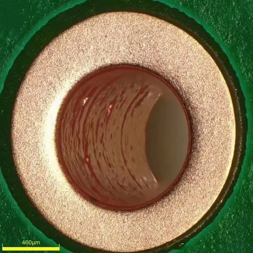
The surface copper remaining around a hole forms its annular land. It links the hole-wall copper with the surrounding pad and trace. Hole position and pad geometry therefore matter alongside the copper deposited inside the hole.
A drill-position shift reduces the remaining copper on one side of the hole while increasing it on the other. Etching also changes the final copper edge. The meaningful connection is the copper that remains after those manufacturing effects, rather than the ideal circular pad shown in the layout editor. A widened trace-to-pad junction can add local copper, yet still leave a narrow connection if drilling removes copper toward that junction. Remaining copper and clearance to the neighboring net need to work together.
For a leaded component, the opening remaining after plating must also fit the lead. Copper deposited on opposite walls reduces the open diameter from both sides of the hole. That is why the finished opening is smaller than the drilled diameter, even though plating has added material to the board. Finished-hole size, lead dimensions and their tolerances determine the fit; the drill tool size and the finished plated diameter are different specifications.
Check the Fabricated Connections
Surface inspection addresses copper-pattern features, pads and the finished board. Bare-board electrical testing checks the intended connectivity and isolation, including the connections between the two faces. Dimensional checks address the relevant outline and holes.
Where the construction calls for examining the plated section, a microsection can reveal the hole-wall copper and its relationship with the laminate and surface copper. It answers a different question from a continuity test. These fabrication checks support the bare board; powered circuit testing follows component assembly.
Double-Sided Boards in Your Product
Control and Interface Boards
A panel connector and a relay may need fixed positions in an enclosure. Routing on the opposite copper face gives their control connections a path around the surface pads and other nets. Plated holes join those routes back to the required connection points, so the electrical layout can work with the mechanical arrangement.
Instrumentation and Sensor Electronics
Analog inputs, signal conditioning and control connections benefit from a layout that makes room for the actual signal and return paths. A two-layer board can serve suitable circuits without adding internal layers. The circuit’s noise, spacing and routing requirements determine the useful construction.
Power and Supporting Circuits
Power conversion and supporting control functions can use two-layer boards where their copper paths, insulation and thermal arrangement fit the application. Current capacity is determined by the conductor construction and operating conditions, rather than by the two-layer label alone.
Bare Boards or a Continued Assembly Build
FLJ can supply the fabricated bare board or coordinate component sourcing, SMT and through-hole assembly. If the product places components on both faces, that adds an assembly sequence to the job; it does not change how the copper-layer count is defined. Our assembly service pages cover the placement, soldering and populated-board test scope.