


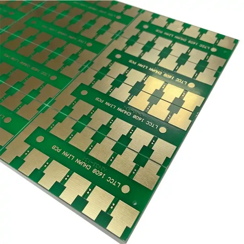
Gold plating here means electroplated gold. It also covers nickel-gold electroplate, electrolytic gold, electro-gold, and electroplated nickel-gold boards. There are two main types of gold plating. One is soft gold. The other is hard gold. Hard gold is often used for gold fingers.
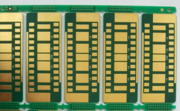
The basic idea is simple. Nickel and gold (often called gold salts) dissolve in a chemical bath. The PCB goes into the plating tank. Then we pass electric current. That makes a nickel-gold layer form on the copper foil of the board. Nickel-gold plating is widely used in electronics. This is because the plated layer is hard, wears well, and resists oxidation.
Why use gold-plated PCBs?
ICs now have more pins. Pins are closer together. Spray tin processes can not make very fine pads flat enough. This makes SMT placement hard. Also tin-lead or HASL boards have a short shelf life. Gold-plated boards solve some of these problems.
For surface mount technology, and for very small parts like 0201 and smaller, pad flatness matters a lot. Pad flatness affects the quality of solder paste printing. That then affects the quality of reflow soldering. So full-board gold plating is common for high-density and very small SMD work.
In the trial or prototype stage, parts buying can delay assembly. Sometimes SMT cannot start for weeks or months after the PCB is made. Gold-plated boards have a much longer shelf life than tin-lead boards. So many prefer gold-plated boards. Also, in sample runs the cost of gold-plated PCBs is close to tin-lead boards.
As routing gets denser, trace width and spacing reach 3–4 mil. This raises risk of gold wire shorting. As signal frequency goes up, the skin effect becomes more important. Skin effect means high frequency AC current moves near the conductor surface. This changes the way signals travel in plated layers. That can affect signal quality. The skin depth depends on frequency.
So in many designs, gold plating helps with solderability, shelf life, and mechanical wear. But designers must watch for issues like gold wire shorting and signal changes at high frequency.
Hard Gold vs Soft Gold
What is hard gold?
Hard gold means we add other metals to the gold layer. This changes the gold structure. The layer becomes harder. Common metals used are cobalt, nickel, copper, palladium, and indium. In the past, iron, tin, and cadmium were used too. Today cobalt and nickel are common. Small indium is added sometimes to tune the color.
Hardness of the plating depends on alloy content. Connector contacts often have hardness around HV130–220. Some decorative or jewelry plating such as 18k gold can reach hardness around 400. Past alloys like gold-copper-cadmium or modern gold-copper-indium can be very hard.
Hard gold is used where wear resistance matters. For example, connector terminals and decorative parts.
What is soft gold?
Soft gold is pure gold plating. No other metals or elements are added. The layer is softer, about HV70 hardness. Soft gold is good for chip bonding and ultrasonic bonding. The LED industry often uses soft gold for wire bonding.
Plating Sequences for Soft and Hard Gold
Soft gold sequence
Pickling → Nickel plating → Pure gold plating
Hard gold sequence
Pickling → Nickel plating → Pre-gold (flash gold) → Electroplate gold-nickel or gold-cobalt alloy
These sequences are standard steps on the shop floor. They ensure the nickel underlayer and then the gold finish. The pre-gold step helps adhesion and final hardness control for the hard gold process.
Difference Between Immersion Gold and Electroplated Gold
Below are practical differences engineers often see. Choose the process based on product needs.
Crystal structure and thickness differ. Immersion gold (often called ENIG in industry) and electroplated gold form different crystal structures. According to the note here, immersion gold tends to be thicker and shows a more golden color. Customers may prefer that look.
Immersion gold is easier to solder in practice. It tends to cause fewer soldering defects and fewer customer complaints. Immersion gold also shows less stress. For products that need bonding, immersion gold can be more suitable. But because immersion gold is softer than electroplated hard gold, immersion gold is not as wear resistant for gold fingers.
As long as pads have nickel underlayer, the skin effect signal path stays in the copper. So immersion gold should not harm signal transmission.
Immersion gold is said to have a denser crystal structure and resists oxidation better. Choose the process by product needs.
With denser routing, trace width and spacing down to 3–4 mil, electroplated gold can more easily cause gold wire short circuits. Immersion gold, with nickel under the pads, avoids gold wire shorting in many cases.
Immersion gold pads with nickel underlayer bond better to solder mask and copper. This makes mask adhesion firmer. When engineers do compensation or rework, distance does not easily change.
Immersion gold is often used for boards with higher flatness and critical assembly needs. It usually does not show black pad problems after assembly. Flatness and shelf life of immersion gold are comparable to good electroplated gold in many cases.
Note: These points reflect practical shop experience. Always test for your specific product and assembly line.
PCB Surface Gold Plating Process Flow
Below are example flows for full-board electroplated hard gold. The values and steps follow a shop standard.
Full-board electroplated hard gold, gold thickness ≤ 1.5 μm
Quy trình
Pre-process → Outer layer dry film → Dry film check → Pattern plating copper-nickel-gold → Secondary dry film → Dry film check → Electroplate hard gold → Outer layer etch → Next process
Production notes
Use GPM-220 dry film that resists electro-gold.
If the full board has no solder mask printing, a second dry film is not needed.
If the board has solder mask, the second dry film should only cover the pad window positions. Do not apply the second film to the whole board.
The secondary dry film film (film for dry film) should act like the solder mask film. Keep only the pads, and do not share the same film as the solder mask film. The dry film must be 2 mil larger than the solder mask film.
Gold thickness 1.5 μm < gold thickness ≤ 4.0 μm
Quy trình
Pre-process → Outer layer dry film → Dry film check → Pattern plating → Outer layer etch → Secondary dry film → Dry film check → Solid plate copper-nickel-gold → Electroplate hard gold → Strip lead wires → Next process
Production notes
Use GPM-220 dry film for electro-gold.
If no solder mask is printed on the full board, second dry film is not needed.
If there is solder mask, second dry film only at the pad windows. Do not do whole board.
Secondary dry film should keep only pads and cannot share with solder mask film. It must be 2 mil larger than the solder mask film.
For gold-plated area spacing, refer to routing capability design.
Use peel-off lead wires or rework lead wire methods.
Special notes
Thick gold plating now often uses gold-cobalt alloy. This is common for PCB plugs or contact switch pads.
For full-board thick gold, evaluate whether thick gold areas have SMT or BGA pads. If so, warn the customer of possible solderability issues. For those positions, suggest pattern-plated copper-nickel-gold instead.
If the customer already prepared lead-out pads that need hard gold, after the outer layer etch you can follow the hard-gold process directly.
Do not make boards with gold thickness > 4 μm.
For processes that use secondary dry film for gold + hard gold, the spacing requirements vs gold thickness are: for gold thickness 0.38 μm min spacing 7 mil; for 0.8 μm min spacing 8 mil; for ≥1.0 μm min spacing 10 mil.
Full-board Electroplated Soft Gold (Gold thickness ≤ 1.5 μm)
Quy trình
Pre-process → Outer layer dry film → Dry film check → Pattern plating copper-nickel-gold → Secondary dry film → Dry film check → Electroplate soft gold → Outer layer etch → Next process
Production notes
Use GPM-220 dry film resistant to electro-gold.
If full board has no solder mask printing, no second dry film is needed.
If board has solder mask, second dry film only for pad windows, not whole board.
Secondary dry film film equals solder mask film. Keep only the pads. Do not share with solder mask film. It must be 2 mil larger than the solder mask film.
Gold thickness 1.5 μm < gold ≤ 4.0 μm
Quy trình
Pre-process → Outer layer dry film → Dry film check → Pattern plating → Outer layer etch → Secondary dry film → Dry film check → Pattern plating copper-nickel-gold → Electroplate soft gold → Strip lead wires → Next process
Production notes
Use GPM-220 dry film resistant to electro-gold.
If full board has no solder mask printing, no second dry film is needed.
If board has solder mask, second dry film only for pad windows.
Secondary dry film must keep only pads and not share with solder mask film. It must be 2 mil larger than solder mask film.
For gold area spacing, follow routing capability design.
Use peel-off lead wires or repair lead wire methods.
Special notes
If customer already has lead-out pads that need soft gold, after outer layer etch follow the soft-gold process.
Do not make boards with gold thickness > 4 μm.
For gold + soft gold using secondary dry film, spacing rules vs gold thickness are: 0.38 μm min spacing 7 mil; 0.8 μm min spacing 8 mil; ≥1.0 μm min spacing 10 mil.
Nickel-free Electroplated Gold (Hard / Soft Gold)
Requirements and notes
For nickel-free gold requested by customer, whether hard or soft gold, the minimum gold thickness must be controlled to 0.5 μm. If less than 0.5 μm, do not use nickel-free gold.
If gold thickness > 4 μm, do not make.
For boards that have nickel electroplated hard or soft gold, follow the same rules. The only difference is do not mark MI as “only gold no nickel”. Instead fill in the required nickel thickness.
For gold + hard gold with secondary dry film, the spacing rules are: 0.38 μm gold min 7 mil; 0.8 μm min 8 mil; 1.0 μm and above min 10 mil.
Design Requirements and Notes for Gold Plating
When there are lead wires
Add a 12 mil wide trace at the end of the gold finger as a lead. For finished copper thickness ≤ 2 oz, if the copper thickness is > 2 oz, the lead trace should not be less than the board’s minimum line width. On both sides of the gold finger, at the nearest milling slot, add a fake gold finger to divide current. This helps prevent uneven thickness in the middle gold fingers.
When there are no lead wires (local electro-thick gold)
Drilling: Drill only PTH holes that go through the board. For NPTH holes use two-drill method processing.
Solder mask 1: MI remarks should state to use electro-gold film.
Marking 1: MI remarks state no marking, only bake the board.
Solder mask 2: MI remarks state to remove solder mask. After removing solder mask, quickly move to next process to avoid oxidation.
Attention
I. The routing film must mask positions that will be electro-gold plated.
II. For electro-gold pads connected to traces, add a teardrop at the pad-to-trace join.
III. Solder mask 2: MI remarks state electro-gold surface must not be sanded. For single-side electro-gold note to only sand large copper side in front-end cleaning.