
Electrolytic Gold Plating for PCBs
Hard and soft gold finishes for electrical contacts and specified bonding surfaces.
FLJ manufactures gold-plated PCBs with nickel or nickel-free constructions, selective plated regions and full-board finishes. We coordinate the gold build with the board circuitry and separate assembly areas.
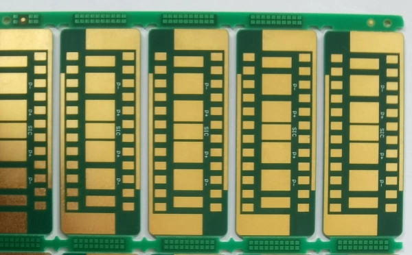
Hard and Soft Gold for Different PCB Interfaces
FLJ supplies hard and soft electrolytic gold for surfaces that perform different connection tasks. Select the deposit for the interface, then specify its thickness and underlying metal stack. A thicker gold layer does not, by itself, make the deposit hard.
| Gold type | Deposit character | Typical interface |
|---|---|---|
| Hard gold | Gold with intentional hardening additions | Mechanically engaged electrical contacts |
| Soft gold | High-purity gold without intentional hardening additions | Specified bonding surfaces |
Hard Gold for Repeated Electrical Contact
Insertion, wiping and switch operation apply mechanical wear to a conductive surface. Hardening additions change the gold deposit’s structure, improving its resistance to that wear. We plate selected contact regions, including board-edge contacts and switch pads, while keeping the finish appropriate to the surrounding circuitry.
For gold-finger edge connectors, the contact finish works with the finger geometry and mating connector. Gold thickness and the supporting metal layers contribute to the contact design; neither alone establishes a service-life rating.
Soft Gold for Specified Bonding Surfaces
Bonding places different demands on the surface. High-purity soft gold avoids the intentional hardening additions used for wear contacts and provides a surface selected for the specified bonding process. FLJ manufactures boards with this electrolytic finish on the designated pads. The bond method and underlying stack determine the required surface condition and coating build.
Nickel Underlayers and Nickel-Free Options
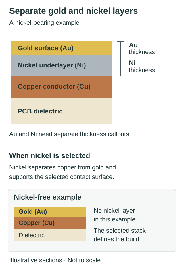
Nickel is a separate construction choice. In a copper–nickel–gold stack, the nickel underlayer helps limit copper diffusion and supports the contact surface. We also supply nickel-free hard- and soft-gold options. Specify gold and nickel thickness separately where nickel is included; PCB thickness describes a different dimension.
ENIG uses electroless nickel and immersion gold. It is a different deposition route, rather than another name for electrolytic soft gold.
Selective Gold Plating and Full-Board Manufacturing
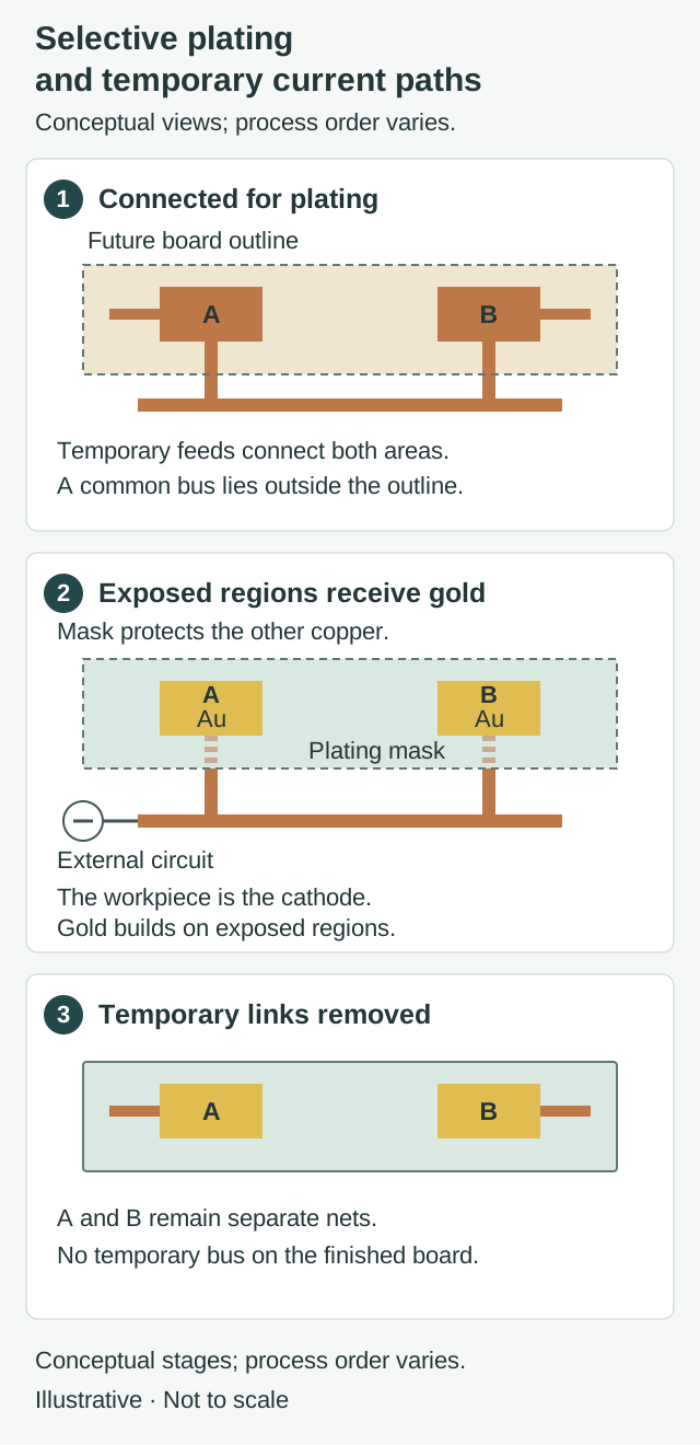
FLJ manufactures plated contact and bonding regions alongside the board’s functional circuitry. Electrical feeds give the selected areas access to the plating circuit, while masks control where metal is deposited. These processing connections are removed from the finished design.
Electrical Feeds and Plating Masks
An isolated pad needs an electrical path to receive an electrolytic deposit. We arrange temporary feeds and plating buses for the selected features, then open the mask over the regions that require gold while protecting other copper. The workpiece is connected as the cathode; the external circuit supplies electrons for gold deposition on its exposed conductive surfaces.
For full-board gold plating, the specified exposed conductive areas receive the finish. The term does not mean that the insulating substrate or protected surfaces are coated with gold.
Underlayer Deposition and Gold Build
Copper preparation removes surface contamination and oxides before the specified metal stack is formed. The selected underlayer, where used, and the hard- or soft-gold deposit establish the required exposed surface.
Current and processing time affect deposited thickness, while the feature pattern and feed arrangement influence how current reaches individual areas. Additional masking and the position of outer-layer etching vary with the gold build and fabrication route; selective thickening is not a single fixed sequence for every board.
Removing Temporary Connections and Finishing the Board
The illustration distinguishes a common plating bus from the intended final circuit. Once that temporary connection has served its purpose, we remove it and check for conductive remnants that could bridge separate nets. Finished contact areas retain their gold surface while the required electrical separation is restored.
Mechanical contacts need a wear-resistant gold surface that remains available for repeated engagement. During soldering, gold can dissolve into the solder, making the underlying metal and solder system part of the joint. We use different finishes on separate board regions to give contact areas and soldering lands the surfaces their connection tasks require.
Electrical connection checks and coating checks address different results: continuity alone does not establish gold thickness, deposit hardness or contact wear life.
Gold Thickness and PCB Manufacturing Capabilities
Supported Gold Plating and Board Constructions
FLJ supplies electroplated-gold rigid boards, flex circuits and rigid-flex constructions. For flex and rigid-flex builds, available regional combinations include electroplated gold with ENIG or OSP, separating plated contact areas from assembly lands.
| Processing parameter | Capability |
|---|---|
| Maximum processing size | 450 × 500 mm |
| PCB thickness | 0.3–5.0 mm |
These values describe the hard-gold processing route. Gold thickness, nickel thickness and PCB thickness remain separate drawing callouts, each tied to its own physical layer.
Gold Build and Selective-Mask Spacing
The gold build also affects manufacturing order. Our hard- and soft-gold route examples for Au ≤1.5 µm place selective thickening before outer-layer etching. Routes for 1.5 < Au ≤4.0 µm place outer-layer etching before secondary masking and subsequent gold build. These are distinct process windows, rather than one coating range for every construction.
Where secondary dry film defines individual hard- or soft-gold regions, spacing must accommodate that masking operation. The following minimum separations apply to those gold regions:
| Au thickness | Minimum region spacing |
|---|---|
| 0.38 µm | 7 mil |
| 0.8 µm | 8 mil |
| ≥1.0 µm | 10 mil |
Within these secondary-film routes, the separations apply to the plated gold regions. General PCB routing and connector-finger pitch use their own requirements.
Finished bare boards can also continue into SMT assembly, with solder-paste printing, component placement and reflow on the designated assembly lands.