


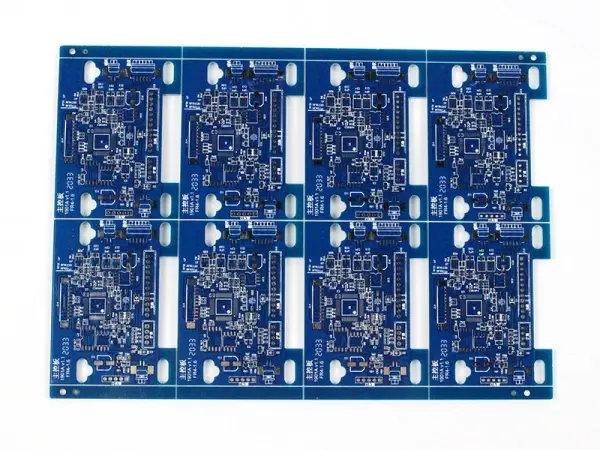
What is an HDI PCB
An HDI board is a high density interconnect printed circuit board. It uses micro blind and buried vias. These boards have a high line density. They have inner layer traces and outer layer traces. They also use drilled holes and plated holes to link traces between layers. As electronic products get smaller and more precise, makers ask for denser PCBs. The best way to increase PCB density is to cut the number of through-holes and to add well-placed blind and buried vias. This need led to the HDI board.
IPC definition
IPC-2226 gives a clear rule for blind and buried vias:
-
Via or buried via diameter ≤ 0.15 mm (0.00591 in).
-
Annular ring diameter ≤ 0.35 mm (0.0138 in).
-
These vias can be made by laser or mechanical drilling, or by dry/wet etching, or by pattern transfer. Then a conductive plating covers the hole.
Note: If the hole diameter is > 0.15 mm (0.00591 in), treat it as a through-hole under the same standard.
Common drilling sizes for HDI
Common via sizes for HDI are 3–5 mil. Designers most often use 4 mil as a middle value for design and production.
Common IPC standards used for HDI
Typical IPC standards for HDI work include:
-
IPC/JPCA-2315 — Guide for high density interconnect structure and microvia design.
-
IPC-2226 — Design standard for high density interconnect (HDI) printed circuit boards.
-
IPC/JPCA-4104 — Specification for dielectric material validation and performance for HDI structures.
-
IPC-6016 — Specification for qualification and performance for HDI structures.
HDI routing: challenges and tips
What HDI routing means
HDI routing means using the latest design ideas and manufacturing methods to make a denser layout without changing the circuit function. In short, HDI uses more routing layers, smaller traces, smaller vias, smaller pads, and thinner cores. This lets you fit complex and often high-speed circuits into spaces that were not possible before.
As the manufacturing methods get better, HDI routing appears in many designs. You will find HDI in motherboards, graphics cards, phones, and other devices with little space. If you do HDI right, you can shrink the board size and also cut EMI problems on the PCB. Lowering cost is a key goal for many companies. HDI routing helps reach that goal.
HDI routing and microvias
HDI routing is more complex than normal multi-layer routing. You might know how to design 8-layer or 16-layer PCBs. Still, HDI introduces new ideas you must learn.
In a normal PCB, we view the whole board as one item with many layers. In HDI, designers must think of many ultra-thin layers stacked to form one board. The main driver for HDI routing is the via technology. Vias are no longer only the plated holes drilled through the finished stack. Traditional through-holes reduce the space available for routing on each layer.
Traditional vias are not fit for HDI
In HDI routing, microvias are the key. They let many dense layers connect together. To explain, microvias look like blind or buried vias but follow a different method. Traditional vias are drilled after the layers are stacked. Microvias are laser drilled on layers before stacking. Laser-drilled microvias allow the smallest hole sizes and pad sizes between layers. This helps with BGA fan-out layouts where pins sit in a grid.
HDI routing strategies
With microvias, PCB designers can route complex networks on many layers. This method is sometimes called “any-layer HDI” or “per-layer interconnect.” Because microvias save space, both outer layers can host dense parts while most routing sits on inner layers.
Low impedance ground planes are vital
When parts and traces get denser in a multilayer board, the risk of EMI and magnetic coupling rises. For HDI design you must ensure the stack has the right structure. Provide enough ground planes to give low impedance return paths.
Place inner routing layers between ground or power layers to cut cross-coupling and crosstalk. Keep high-speed signal paths short and keep their return paths short too. Plan microvias so they limit signal paths to a small area. This reduces EMI risk.
For safety, use proper simulation tools to model the HDI PCB before production.
Main benefits of HDI PCBs
Many people want to reduce product size. One of the best ways is to use HDI PCBs. When you need less weight and smaller size but keep function and reliability, HDI is a good solution.
Key benefits:
-
HDI allows pad-in-pad and blind via use. This lets parts sit close and cuts trace length. Shorter traces often mean faster and more reliable signals.
-
These boards can give good performance at a fair cost. HDI is an affordable choice for people who need reliable, durable electronics.
-
To decide if HDI fits your project, learn more about them and how to use them. Know the differences between normal PCBs and HDI PCBs.
Where HDI PCBs are used today
Because of their benefits, HDI PCBs appear in many fields.
-
Medical devices — Many medical tools must be small. Lab gear and implants often need tiny boards. HDI helps here. A pacemaker is a good example. Many monitoring and probe tools, like endoscopes, use HDI too. In these cases, smaller is better.
-
Automotive — Cars use space well. Some car electronics are getting smaller. HDI helps reduce size while keeping function.
-
Mobile devices — Tablets and phones use HDI. This is why these devices become thinner as they evolve.
-
Aerospace and defense — These fields use HDI for its reliability and small size. HDI shows up more as new designs need compact and stable boards.
Many other fields will use more HDI in the future.
What makes an HDI PCB an HDI PCB
An HDI PCB uses blind via plating and then a second lamination step. These boards can be first level, second level, third level, and higher. Makers usually build HDI boards by lamination steps. The more lamination steps, the higher the technical level.
-
Basic HDI boards often use one lamination step.
-
Higher level HDI uses two or more lamination steps.
-
High-level HDI may use stacked vias, plated filled vias, laser direct drilling, and other advanced methods.
Now we explain common layer stacks and how producers build them.
Simple single-laminate HDI (example)
A simple single-laminate HDI board can be a 6-layer board with a 1+4+1 stack. This board is simple. The inner multi-layer board has no buried vias. One lamination completes the board. The manufacturing is similar to normal multilayer single-laminate boards. But after lamination you still need laser drilling for blind vias and other steps.
Normal single-laminate HDI (common case)
A common single-laminate HDI has a structure (1 + N + 1) where N ≥ 2 and N is even. For example, a single-laminate 6-layer HDI uses 1+4+1. This structure is the mainstream design for single-laminate HDI. The inner multi-layer often has buried vias that require a second lamination step to finish. This single-laminate type often has blind vias and buried vias. If designers can change this type into the simple single-laminate form above, both buyer and supplier benefit.
Normal double-laminate HDI (common case)
A common double-laminate HDI might be an 8-layer board with a 1+1+4+1+1 stack. This stack is (1+1+N+1+1) with N ≥ 2 and even. This is the mainstream double-laminate design in the PCB industry. The inner multi-layer has buried vias that need three lamination steps. This type often does not have staggered via stacks. If you can change buried vias from layers 3–6 to layers 2–7, you can reduce one lamination step and cut cost.
Another common double-laminate HDI
This type also uses (1+1+N+1+1). Even though it is a double-laminate structure, the buried via sits in a different place — between layers 2 and 7. This change can reduce lamination steps from three to two. But this design has one hard point: it can create blind vias from layers 1–3. You must split those into two sets (1–2 and 2–3) and make the 2–3 inner blind vias with via filling. Via filling adds cost and difficulty. So during design, try to avoid stacked vias and change 1–3 blind vias into staggered 1–2 and 2–3 blind and buried vias.
Uncommon double-laminate HDI with cross-layer blind vias
One uncommon double-laminate HDI 6-layer board uses 1+1+2+1+1. It still uses the (1+1+N+1+1) idea with N ≥ 2 and even. This design has cross-layer blind vias. The blind via depth grows — a 1–3 depth blind via is twice the depth of a normal 1–2 blind via. Customers who choose this design have specific needs and do not want the blind via split into stacked vias. These cross-layer blind vias are hard to drill by laser. Copper deposition and plating on such deep blind vias are also difficult.
Stacked blind via design in double-laminate HDI
There is a type where buried vias at layers 2–7 need stacked blind vias above them. This is still a (1+1+N+1+1) structure. Some double-laminate HDI boards use this method. The inner multi-layer has buried vias and needs two lamination steps. The key is that the stacked via design adds difficulty. But placing buried vias at layers 2–7 reduces one lamination step and saves cost.
Cross-layer blind via design in double-laminate HDI
Another double-laminate (1+1+N+1+1) design includes cross-layer blind vias. This design is harder to make and some HDI makers lack the skill. The inner multi-layer has buried vias in layers 3–6 and needs three lamination steps. The main issue is the cross-layer blind via design. If you can split the 1–3 cross-layer via into 1–2 and 2–3 blind vias, the cost drops and the process becomes simpler. Note: this split differs from the stacked-via split explained earlier. This split uses staggered blind vias instead of stacked blind vias.
Levels of HDI
-
First-level (1st order) HDI is simple. The process and control are easier.
-
Second-level HDI is more complex in production and manufacturing.
-
Third-level and above follow the second-level rules but are more complex.
Differences between HDI and regular PCBs
HDI boards are often made by lamination techniques using thin core materials. The more laminations, the higher the process level. Most HDI boards use one lamination. High-level HDI uses two or more lamination techniques and adds advanced methods such as stacked vias, plated filled vias, and laser direct drilling.
When the relative density of a PCB gets higher than an eight-layer board, making it by HDI often costs less than doing complex traditional lamination and pressing. HDI boards often have higher mechanical strength and better signal accuracy than traditional PCBs.
Other improvements of HDI over regular PCBs:
-
Better performance for microwave and RF signals.
-
Better resistance to radio interference and electrostatic discharge.
-
Better heat conduction.
High-density integration (HDI) allows end products to be smaller and more standard in function and performance.
Simple advice for designers and buyers
-
Use HDI when you need smaller size and better performance.
-
Talk to your PCB supplier early. HDI needs design-for-manufacture (DFM) checks.
-
Ask for IPC-based specs. Use IPC-2226 and IPC-6016 where possible.
-
Plan stackups with enough ground planes to keep return paths short.
-
Use microvia sizes that match your PCB house capability. Common: 3–5 mil, often 4 mil.
-
Try to avoid stacked vias unless necessary. Staggered blind/buried vias are often easier.
-
If you choose multi-step lamination HDI, expect more process steps and inspection.
-
Use proper simulation for high-speed or RF designs to check EMI and signal integrity.
-
For BGA fan-out, microvias and pad-in-pad help reduce fan-out area and trace length.
-
For cost control, reduce the number of lamination steps when you can. Optimize via placement.
Closing summary
HDI boards are high density interconnect PCBs that use micro blind and buried vias. They let designers pack more traces and parts into less space. HDI routing calls for careful stackup planning, good ground planes, exact microvia use, and proper DFM checks. HDI gives clear benefits on size, signal speed, and performance. HDI appears in many fields, from medical and mobile to automotive and aerospace. The more complex the HDI level, the more advanced the process and the higher the cost. Good design and early supplier communication will help you get the right HDI board for your product.