
HDI PCB Manufacturing
Build compact electronics around connections that fit the package. FLJ manufactures high-density interconnect (HDI) PCBs with laser microvias, fine circuit features and sequential build-up structures for prototypes and production.
Choose the build-up, material, copper and finished surface around the component layout and electrical requirements. Bare-board fabrication can continue into component sourcing, assembly and testing through FLJ.
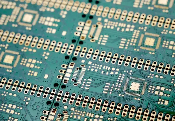
HDI Build-Up Options for Your Board
An HDI board creates routing space through smaller interconnect features and selective connections between layers. The difference is the way the layers connect, rather than a particular total layer count. A conventional eight-layer board and an eight-layer HDI board can have different via structures and fabrication routes. In the build-up notation below, N is the copper-layer count of the middle sub-board.
1+N+1: one build-up layer on each side
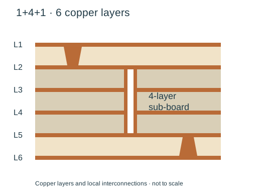
The middle N-layer sub-board carries the internal circuitry. A dielectric region and an additional copper layer are added on each side, with microvias connecting the added surface layers to the layers immediately beneath them. The sub-board can also contain buried interconnections formed before the outer build-up is added.
A 1+4+1 example has six copper layers in total. This structure can provide a shallow connection below a fine-pitch device while retaining a conventional internal sub-board. The actual construction defines which layers connect and how other through connections are formed.
2+N+2: two build-up layers on each side
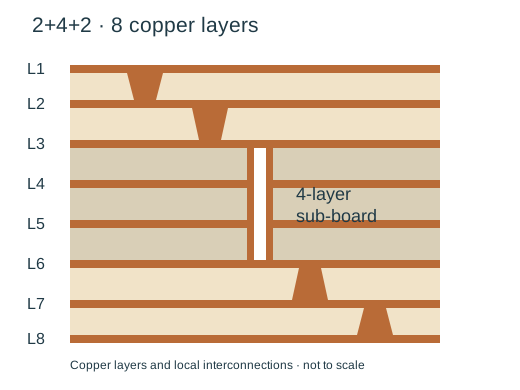
A second build-up layer on each side adds another level of microvia interconnection. For example, a 2+4+2 board has eight copper layers. The additional connection level can move an escape route farther into the board while reserving other areas for routing.
The numbers describe copper-layer construction, not signal, ground and power assignments. They also do not specify a complete production sequence on their own. Dielectric thicknesses, via locations, filling and the internal sub-board determine how the structure is fabricated.
Illustrative constructions, not production stackup drawings. Copper, dielectric and connection spans are shown without manufacturing dimensions; individual nets and clearances are omitted.
Staggered or stacked microvias
Staggered microvias occupy different positions on successive layers and connect through the intermediate copper pattern. Stacked microvias align the connections vertically. Stacking can reduce the lateral space used by the connection, while adding another interface at the landing below the upper microvia.
In a copper-filled stacked structure, the upper microvia lands on the copper over the lower one. Cleaning that landing surface and forming the next deposited copper connection are part of making the vertical path. The interface between build-up levels matters as much as the visible alignment. Higher-order and any-layer structures extend the connection choices; they are selected for the actual escape and fabrication needs rather than as a general quality ranking.

More Routing Space Around Fine-Pitch Components

A through via occupies a drilled path through the board, including layers where that connection is not needed. Its pads and clearances can interrupt escape channels around a dense device. A microvia ending at a nearby layer leaves the deeper layers available for other routes.
This is useful around high-pin-count processors, FPGAs and compact communication modules, where many signals must leave a small component footprint. Moving a connection below the surface can open a different path through the pad field. The benefit depends on the component pitch, usable routing channels, pad dimensions and the layers needed by each net.
Via-in-pad places the connection within the component land. A filled and capped pad provides a continuous surface for assembly instead of leaving an open hole that can draw solder from the joint. Pad planarity and the selected filling and capping process are part of that construction.
HDI can shorten some connections and avoid unnecessary via length. Return-path continuity, controlled impedance, material losses and the remaining interconnect geometry still determine electrical behavior. The useful choice is the structure that connects the device and preserves the intended signal path.
Manufacturing the Microvia Connection
Form the internal sub-board
FLJ fabricates the inner circuits and required buried connections before adding the outer build-up. The accessible circuit patterns are inspected before they are enclosed. Those inner layers also establish the copper landing pads that subsequent microvias must reach.
Add the dielectric and create the connection
New prepreg or another suitable build-up dielectric bonds the next copper layer to the sub-board. Its resin must fill the spaces around the existing copper pattern and form the intended insulation thickness. Copper distribution, dielectric selection and the press process work together to achieve that bond.
The laser process opens the microvia to its target copper. FLJ prepares the hole and landing surface, then forms the conductive connection through metallization and copper deposition. Residue at the hole bottom can interrupt the bond to the target pad, so hole preparation and deposition belong to the same connection process. Where the structure calls for a filled microvia, copper filling and surface preparation create the landing for another build-up connection or the finished pad.
Further build-up repeats the necessary operations around the partially completed board. Each previously formed structure experiences the later thermal history, so material adhesion and the connection interfaces must suit the complete route through fabrication and assembly.
Check the connection beyond its initial appearance
Interconnect checks address the actual structure: optical inspection of accessible copper patterns, registration of holes to landing pads, and the condition of deposited copper and filling. A cross-section through a representative feature exposes its local geometry and connection interface, including details hidden by the finished surface.
Electrical testing checks continuity and isolation against the board’s circuit data. Initial continuity is different from evidence that an interconnect will remain intact through thermal or environmental stress. Where the application needs that evidence, representative structures and an appropriate qualification plan can be used to evaluate the build under the relevant conditions.
Materials, Fine Lines and Assembly Surfaces
| Option | How it fits the build |
|---|---|
| Build-up dielectric | The dielectric system sets the physical depth of the microvia and contributes to the finished spacing between copper layers. Resin content and flow must match the copper pattern being enclosed; simply choosing a thinner sheet does not complete the construction. The cured inner layers remain part of the board while newly added material supplies the resin for the next bond. Material selection also accounts for repeated fabrication and assembly heat, dielectric properties relevant to the circuit, and the operating environment. In glass-reinforced material, moisture and electrical bias can support conductive anodic filament (CAF) growth along internal glass/resin interfaces. That internal path differs from surface electrochemical migration. Material resistance to the relevant environment and conductor separation are considered together. |
| Copper and circuit geometry | Fine lines need a copper build and imaging and etching process that can produce the intended conductor shape and separation. The finished copper includes the effects of subsequent deposition, not only the starting foil. Local pads, annular features and the layer-to-layer registration allowance must fit the same interconnect plan. Finished thickness and mechanical support also matter around press-fit connectors, fasteners and test fixtures. Supporting the board near concentrated loads limits local deflection during assembly and use. |
| Surface finish and clean assembly lands | ENIG, OSP and other suitable finishes protect exposed copper and provide an assembly surface. Selection follows the pad geometry, soldering route, storage needs and any additional connection processes. Surface finish, conductive microvia filling and copper capping perform different jobs. Moisture, electrical bias and ionic residues can support electrochemical migration between close conductors. Cleanliness control belongs alongside the finish and assembly process; a surface-finish name alone does not establish environmental reliability. |
Choosing an HDI Build for Prototype and Production
Compare HDI with a conventional multilayer construction when through-via geometry limits escape routing, board area or the required connections. An added build-up level is useful when it solves a connection problem. More levels alone do not make the finished board a better fit.
The complete construction determines cost: internal sub-board, number of build-up stages, hole formation and filling, materials, fine circuit features, panel utilization, quantity and verification scope. A smaller board or fewer routing layers may offset some additional processing. For the same board envelope, a viable 1+N+1 escape scheme can be compared with a 2+N+2 alternative to see whether the extra connection level is needed. Each alternative includes its own dielectric, filling and verification requirements; layer count alone does not settle the comparison.
A prototype can establish the selected construction and support circuit and assembly evaluation. Production carries forward the defined stackup, materials, interconnections and inspection requirements. If a change affects the connection route, material system or thermal exposure, it is assessed with the affected parts of the build.