


مقدمة
عندما تخضع لوحة الدوائر المطبوعة (PCB) لعملية لحام إعادة التدفق، فإنها غالبًا ما تنحني أو تلتوي. إذا كانت المشكلة خطيرة، يمكن أن ترتفع الأجزاء، أو يمكن أن تفشل وصلات اللحام، أو يمكن أن تقف المكونات على نهايتها. تشرح هذه المقالة أولاً مخاطر اعوجاج ثنائي الفينيل متعدد الكلور. بعد ذلك، يبحث في الأسباب الرئيسية للالتواء. وأخيرًا، يسرد طرقًا عملية لتقليل الاعوجاج أو منعه. تابع القراءة لمعرفة الخطوات والأسباب الواضحة والبسيطة.
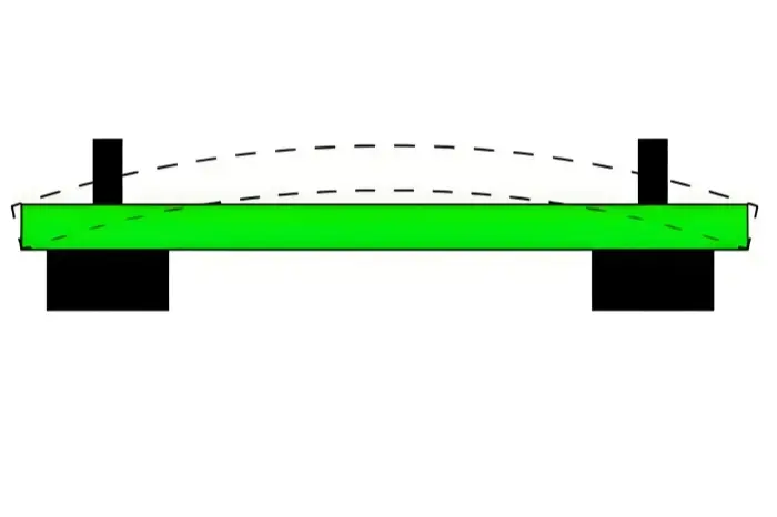
مخاطر تشوه ثنائي الفينيل متعدد الكلور
إذا لم يكن ثنائي الفينيل متعدد الكلور مسطحًا على خط تركيب السطح الآلي، فقد لا تضع الماكينة الأجزاء في المكان الصحيح. قد لا تدخل الأجزاء في الثقوب أو تهبط على وسادات SMD. في بعض الحالات، يمكن أن تتلف ماكينة الإدخال الآلي. بعد تركيب الأجزاء ولحامها، فإن اللوحة المشوهة تجعل من الصعب تقليم الأسلاك بشكل نظيف. قد لا تتلاءم اللوحة مع العلبة أو يتم توصيلها بالمقابس. لذلك تجد محلات التجميع أن الاعوجاج مشكلة كبيرة.
تتحرك تقنية التركيب السطحي (SMT) نحو دقة أعلى وسرعة أعلى والمزيد من الأتمتة. وهذا يزيد من الحاجة إلى تسطيح مركبات ثنائي الفينيل متعدد الكلور. إن التسطيح مهم لأن الماكينات الحديثة تتوقع أن تكون اللوحة مستقرة ودقيقة أثناء التركيب واللحام.
من الناحية العملية، تنص معايير IPC على أن الحد الأقصى المسموح به للالتواء المسموح به للوحات المزودة بأجهزة مثبتة على السطح هو 0.75%. أما بالنسبة للألواح التي لا تحتوي على أجهزة مثبتة على السطح، فإن الحد الأقصى هو 1.5%. تضع بعض الشركات حدودًا أكثر صرامة لتلبية التجميع عالي السرعة والدقة. على سبيل المثال، يطلب بعض العملاء حد أقصى للالتواء يبلغ 0.5% أو حتى 0.3%.
ما الذي يسبب تشوه ثنائي الفينيل متعدد الكلور
يتكون ثنائي الفينيل متعدد الكلور من مواد مختلفة، مثل رقائق النحاس والراتنج والألياف الزجاجية. تعمل هذه المواد بشكل مختلف تحت الحرارة والإجهاد. عندما يتم ضغطها ومعالجتها معًا، يمكن أن يتسبب الإجهاد الحراري المتبقي في حدوث التواء. بالإضافة إلى ذلك، يحتوي تصنيع ثنائي الفينيل متعدد الكلور على العديد من الخطوات التي تضيف الحرارة والحمل الميكانيكي. وتشمل هذه الخطوات التصفيح والحفر والقطع والخبز واللحام. كل هذه الخطوات يمكن أن تغير شكل اللوحة. ونظرًا لأن العديد من العوامل يمكن أن تسبب الاعوجاج، غالبًا ما يكون من الصعب العثور على السبب الرئيسي.
منطقة نحاسية غير مستوية
غالبًا ما تُستخدم المساحات النحاسية الكبيرة في المستويات الأرضية أو مستويات الطاقة. إذا لم تكن هذه المساحات النحاسية الكبيرة موزعة بالتساوي على اللوح، فإن امتصاص الحرارة وإطلاق الحرارة سيكون غير متساوٍ. عندما يسخن اللوح ويبرد، تتمدد أجزاء اللوح وتتقلص بمعدلات مختلفة. يؤدي هذا التمدد غير المتكافئ إلى حدوث إجهاد ويمكن أن يتسبب في تشوه اللوح. إذا وصل اللوح إلى درجة حرارة التحول الزجاجي (Tg)، تلين المادة ويمكن أن يتغير شكلها بشكل دائم.
الشرائح والطبقات
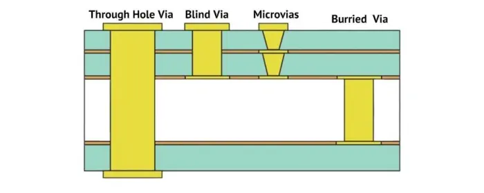
معظم مركبات ثنائي الفينيل متعدد الكلور الحديثة متعددة الطبقات. يتم ربط الطبقات بواسطة فياس. تأتي الفتحات في ثلاثة أنواع: الفتحات العابرة، والفتحات العمياء، والفتحات المدفونة. حيثما تربط الفتحات الطبقات ببعضها البعض، فإنها تحد من كيفية تمدد اللوحة وتقلصها. يمكن أن يسبب هذا القيد إجهادًا موضعيًا ويمكن أن يجعل اللوحة بأكملها تنحني أو تلتوي.
وزن اللوحة ووزن المكونات
غالبًا ما تقوم أفران إعادة التدفق بتحريك مركبات ثنائي الفينيل متعدد الكلور على سلاسل تدعم اللوحة عند الحواف. إذا كانت اللوحة تحتوي على أجزاء ثقيلة جدًا أو كانت كبيرة جدًا، يمكن أن يؤدي وزنها إلى ترهل المركز. يؤدي هذا الترهل إلى تقوس أو انحناء أثناء التسخين ويمكن أن يبقى بعد التبريد.
عمق القطع على شكل حرف V وتصميم علامات التبويب في الألواح
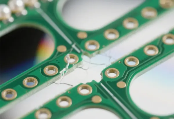
القطع على شكل حرف V هي طريقة لفصل الألواح في اللوح. يقلل القطع على شكل حرف V من القوة الهيكلية في اللوح. المناطق المقطوعة ضعيفة ويمكن أن تلتوي بسهولة أكبر. تزيد عمليات القطع على شكل حرف V العميقة أو العديد من عمليات القطع على شكل حرف V على اللوح الواحد من خطر الالتواء أثناء المعالجة.
اختلافات المواد والتكديس
يُصنع ثنائي الفينيل متعدد الكلور من اللب والرقائق المسبقة والرقائق النحاسية الخارجية. أثناء التصفيح، تسخن النوى والرقائق وقد تتشوه. ويعتمد مقدار التغير على معامل التمدد الحراري لكل مادة (CTE).
تحتوي رقائق النحاس والمادة الأساسية FR-4 على قيم CTE مختلفة. بالنسبة إلى FR-4، يختلف CTE المحور Z تحت Tg عن CTE فوق Tg. أعلى من Tg، يلين الراتنج ويمكن أن يكون التمدد أكبر بكثير. المواد ذات درجة الحرارة العالية تتغير بدرجة أقل في درجات الحرارة العالية وتحافظ على شكلها بشكل أفضل.
عندما يكون للأنوية المختلفة أنماط نحاس أو سمك أو مواد مختلفة، فإنها تتمدد بكميات مختلفة أثناء التصفيح. إذا تم الربط بين قلبين مختلفين للغاية في CTEs عن طريق التصفيح المسبق ومعالجتهما، فقد تنكمش اللوحة في ضغط غير متساوٍ. عندما يبرد اللوح، تتسبب هذه الاختلافات في انحناء اللوح نحو الجانب الذي تقلص بشكل أقل.
التدوير الحراري أثناء التصفيح
أثناء التصفيح، ترتفع درجة الحرارة وترتفع درجة الحرارة وتتدفق المادة المُعدّة مسبقًا وتملأ الأنماط النحاسية ثم تعالج. بينما لا يزال ما قبل التصفيح طريًا، يمكن أن تتمدد النوى بحرية. ولكن بعد المعالجة، تلتصق الطبقات ببعضها البعض. إذا كانت النوى قد تمددت بكميات مختلفة، فإن التجميع المعالج يحمل عدم التطابق. عندما يبرد اللوح، تبقى معدلات الانكماش غير المتطابقة وتتسبب في حدوث تشوه دائم.
خطوات التصنيع التي تضيف الإجهاد
تضيف خطوات عملية ثنائي الفينيل متعدد الكلور كلاً من الإجهاد الحراري والميكانيكي. يأتي الإجهاد الحراري بشكل أساسي من التصفيح. ويأتي الإجهاد الميكانيكي من التكديس والمناولة والخبز. تشمل نقاط العملية المهمة ما يلي:
- الصفائح المكسوة بالنحاس الواردة: هذه تكون متماثلة في الهيكل وعادةً لا تلتوي أثناء التصفيح، ولكن المكبس به اختلافات في درجات الحرارة عبر الصفيحة. يمكن أن تؤدي هذه الاختلافات الموضعية إلى حدوث ضغوط موضعية صغيرة تظهر لاحقًا.
- التصفيح: هذا هو المصدر الرئيسي للإجهاد الحراري. في تكدس ثنائي الفينيل متعدد الكلور، تختلف أنماط الطبقات وكذلك كميات ما قبل التصفيح. هذه الاختلافات تجعل الإجهاد الحراري أعلى ويصعب إزالته. أثناء الحفر والتوجيه والخبز، يمكن أن يتحرر الإجهاد المخزن ويتسبب في اعوجاج اللوحة.
- قناع اللحام والخبز الأسطوري: تعالج أحبار أقنعة اللحام حوالي 150 درجة مئوية. يمكن أن تكون درجة الحرارة هذه أعلى من درجة حرارة المواد ذات درجة الحرارة المنخفضة إلى المتوسطة وتجعل اللوح أكثر مرونة. بينما تكون الألواح على الرفوف في الفرن أو تحت تدفق الهواء، يمكن أن تنحني تحت وزنها أو هواء الفرن. وهذا يزيد من الاعوجاج.
- تسوية لحام الهواء الساخن بالهواء الساخن (HASL): HASL هو حدث حراري سريع. درجة حرارة وعاء اللحام النموذجية عالية وتنتقل اللوحة من درجة حرارة الغرفة إلى حرارة عالية ثم يتم غسلها وتبريدها. تضيف دورة التسخين والتبريد السريع إجهادًا حراريًا ويمكن أن تسبب إجهادًا دقيقًا واعوجاجًا أكبر.
- التخزين والمناولة: غالبًا ما يتم تخزين الألواح عموديًا على رفوف. إذا كانت الرفوف ضيقة للغاية، أو إذا كانت الألواح مكدسة، يمكن أن تنحني بسبب القوة الميكانيكية. تكون الألواح الرقيقة التي يقل قطرها عن 2.0 مم أكثر تأثراً.
كيفية تقليل تشوه ثنائي الفينيل متعدد الكلور
فيما يلي طرق عملية لتقليل الالتواء أثناء إنتاج ثنائي الفينيل متعدد الكلور وتجميعه.
1. خفض درجة الحرارة وبطء التسخين/التبريد
نظرًا لأن درجة الحرارة هي المصدر الرئيسي للإجهاد، فإن خفض درجة حرارة الفرن أو إبطاء معدل التسخين والتبريد في عملية إعادة التدفق يساعد في ذلك. إذا تم تسخين اللوح وتبريده ببطء أكثر، يكون الإجهاد الناتج عن التمدد الحراري أقل ويقل احتمال حدوث التواء. لاحظ أن تغيير ملف تعريف درجة الحرارة قد يؤثر على جودة اللحام أو وقت الدورة، لذا تحقق من الآثار الجانبية.
2. استخدام مواد عالية الجاذبية
Tg هي درجة حرارة التحول الزجاجي. وفوق درجة حرارة التحول الزجاجي تلين المادة وتصبح شبيهة بالمطاط. تلين المواد ذات درجة الحرارة المنخفضة Tg بشكل أسرع ولفترة أطول عند إعادة التدفق. يزيد استخدام المواد الأساسية ذات درجة حرارة Tg الأعلى من مقاومة اللوح للتشوه تحت الحرارة. تكلف المواد ذات درجة Tg العالية أكثر ولكنها تساعد على تجنب الالتواء والمشاكل الأخرى المتعلقة بالحرارة. يشيع استخدام مادة Tg العالية في العمليات الخالية من الرصاص.
3. زيادة سماكة اللوح
تهدف العديد من المنتجات الاستهلاكية إلى الحصول على ألواح ثنائي الفينيل متعدد الكلور رقيقة وخفيفة. فالألواح الرقيقة التي يصل سمكها إلى 1.0 مم أو 0.8 مم أو 0.6 مم شائعة الآن. يصعب الحفاظ على الألواح الرقيقة مسطحة خلال إعادة التدفق. إذا كان المنتج يسمح، استخدم ألواحًا بسُمك 1.6 مم قياسي للوحة 1.6 مم. الألواح السميكة تقاوم الانحناء والترهل وتقلل من مخاطر الالتواء.
4. تقليل حجم اللوحة وعدد الألواح
نظرًا لأن أفران إعادة التدفق غالبًا ما تدعم اللوحة عند الحواف، يمكن أن تتدلى الألواح الكبيرة تحت وزنها. بالنسبة للألواح الكبيرة، حاول توجيه الحافة الطويلة على طول سلسلة الدعم بحيث يتم تقليل الترهل. استخدم أيضًا عددًا أقل من الألواح لكل لوحة عندما يكون ذلك ممكنًا. اجعل اللوح يمر عبر الفرن مع توجيه الحافة الضيقة للأمام لتقليل الترهل.
5. استخدم حاملات أو صواني إعادة التدفق
إذا كانت الطرق الأخرى غير كافية، استخدم حاملات إعادة التدفق أو القوالب. يحافظ الناقل على ثبات ثنائي الفينيل متعدد الكلور أثناء التسخين والتبريد. يحافظ الناقل على اللوحة من الحركة حتى تبرد اللوحة تحت درجة حرارة أقل من Tg وتستعيد صلابتها. إذا كان الناقل من جانب واحد غير كافٍ، فاستخدم حامل من قطعتين يشبك اللوحة بين اللوحين العلوي والسفلي. تكلف الناقلات أموالاً وتتطلب وقتًا إضافيًا في المعالجة، ولكنها تقلل من الاعوجاج بشكل جيد.
6. استبدل V-Cut بعلامات التبويب الموجهة أو “عضات الفأر”
نظرًا لأن القطع على شكل V يمكن أن يضعف اللوحة، قلل من عمق القطع على شكل V أو استخدم ألسنة صلبة أو قضبان موجهة. الألسنة الصلبة أو الثقوب المختومة تحافظ على قوة اللوحة عالية وتقلل من مخاطر الالتواء. عند الحاجة إلى استخدام القطع على شكل حرف V، حافظ على أن تكون القطع سطحية واترك إطار اللوحة كافيًا لدعم اللوح.
7. اختيار المواد بعناية وتناسق التصميم
اختر المواد الأساسية التي لها نفس CTE والتي تتطابق مع احتياجات العملية. تصميم أنماط النحاس لتكون متماثلة قدر الإمكان بين الأعلى والأسفل وعبر الطبقات. تجنب صب النحاس الكبير غير المتوازن على جانب واحد بينما يكون الجانب الآخر متناثرًا. استخدم التقسيمات المستوية الداخلية أو التخفيفات الحرارية لموازنة توزيع النحاس عندما يكون ذلك ممكنًا.
8. استخدام التكديس المتماثل أو المدروس
يقلل التكدس المتماثل (طبقات تشبه المرآة) من عدم التوازن ويقلل من الاعوجاج. إذا كانت هناك حاجة إلى تكديس غير متماثل لأسباب كهربائية، فحاول تخطيط ترتيب الطبقات بحيث يظل الهيكل العام متوازنًا. عند اختلاف المواد الأساسية، يمكن تكييف وضع الطبقات ولوح الأدوات في كومة التصفيح لتقليل الضغط.
9. تحسين معلمات التصفيح
إعدادات التصفيح مهمة: تؤثر إعدادات التصفيح على الإجهاد: يؤثر كل من ملف درجة حرارة المكبس ووقت الانتظار والتحكم في التبريد. استخدم المكابس التي يمكنها التحكم في التبريد في نهاية الدورة الساخنة. تعتبر المكبس الساخن المزود بتبريد متكامل أفضل من المكبس الساخن الذي ينقل المكدس إلى مكبس بارد بسرعة. استخدم أيضًا التكديس المتماثل لألواح الأدوات والمواد العازلة حول كومة ثنائي الفينيل متعدد الكلور أثناء التصفيح.
بالنسبة للألواح التي يجب أن تستخدم مواد غير قياسية أو هياكل غير متماثلة، جرّب التكديس غير المتماثل في المكبس. تكمن الفكرة في وضع المواد العازلة أو ألواح الأدوات بطريقة توازن تدفق الحرارة بحيث يسخن ويبرد كلا الجانبين بسرعات متماثلة. قد يقلل هذا من تأثير عدم تطابق CTE. تساعد أيضًا خطوات المعالجة بعد التصفيح أو خطوات ما بعد الخَبز على استقرار اللوح.
10. تجنب أخطاء رف الفرن والتحكم في تدفق الخبز
عند خبز قناع اللحام أو الأحبار الأسطورية، لا تكدس الألواح بطريقة تسمح للألواح السفلية بالانحناء تحت الوزن. تأكد من أن اتجاه اللوح في الفرن يتطابق مع تدفق الهواء حتى لا تؤدي الرياح إلى ثني الألواح. في التسوية بالهواء الساخن، تأكد من وضع اللوح بشكل مسطح والسماح له بالتبريد قبل 30 ثانية على الأقل قبل الغسيل بالماء لتجنب التبريد المفاجئ الذي يسبب صدمة حرارية.
11. إدارة التخزين والمناولة
قم بتخزين الألواح على رفوف لا تثنيها. تجنب تكديس العديد من الرفوف في مساحات صغيرة حيث تضغط الألواح على بعضها البعض. استخدم مسافات مناسبة بين المنصات والرفوف بحيث لا تتعرض الألواح للضغط والتشوه بسبب اللدونة. قد لا تتم إزالة بعض التشوهات الناتجة عن التخزين بالكامل من خلال خطوات التسطيح اللاحقة.
12. تسطيح ما قبل الشحن (التسطيح النهائي)
تُجري معظم شركات تصنيع ثنائي الفينيل متعدد الكلور خطوة تسطيح نهائية قبل الشحن. يمكن أن تكون هذه الخطوة التسطيح الميكانيكي أو التسطيح الحراري تحت الوزن. نظرًا لأن قناع اللحام وطلاء السطح يؤثران على كيفية عمل التسطيح بالحرارة، تحكم في درجة حرارة الخبز والوقت بعناية. بالنسبة لمعظم الألواح، يساعد التسخين إلى أقل من درجة حرارة Tg أو بالقرب منها واستخدام الوزن أثناء التبريد على تسطيح الألواح. بالنسبة للمواد ذات درجة الحرارة المرتفعة Tg، قد تحتاج إلى درجات حرارة أعلى ولكن راقب حدود الحبر والطلاء.
تساعد زيادة الضغط أثناء الخَبز وإبطاء وقت التبريد بعد الخَبز على تأثير التسطيح. يجب أن تتطابق هذه الإعدادات مع مادة اللوح والطلاء. يمكن أن يقلل التسطيح النهائي من الاعوجاج بشكل كبير ولكنه ليس إصلاحًا كاملاً إذا تسببت خطوات المعالجة السابقة في إجهاد مدمج كبير.
ملاحظات الإنتاج والتصميم
عندما تستخدم اللوحة مادة منخفضة الزئبق، يميل معدل عيوب الالتواء إلى أن يكون أعلى من المواد عالية الزئبق. وعادةً ما تشتمل المواد عالية الزئبق على مواد مالئة ولها CTE أقل من الأنواع منخفضة الزئبق. أثناء المعالجة النهائية، تؤثر درجة حرارة الخَبز المعتادة بالقرب من 150 درجة مئوية على الألواح منخفضة الزئبق أكثر من الألواح منخفضة الزئبق.
في التصميم، تجنب عدم التناسق الهيكلي، وعدم تناسق المواد، والنقش النحاسي غير المتساوي. تزيد مشكلات التصميم هذه من مخاطر الالتواء. أيضًا، غالبًا ما يؤدي التصفيح من قلب إلى قلب (ربط عدة أنوية مباشرةً) إلى إجهاد أكثر تعقيدًا من التصفيح أحادي النواة مع تصفيح رقائق النحاس. تُظهر المداخن الأساسية التي تحتوي على ثلاثة أنوية أو أكثر معدل فشل أعلى في اختبارات الاعوجاج من الهياكل الأبسط.
يؤثر تصميم إطار اللوحة أيضًا على الالتواء. يمكن للإطار النحاسي الكبير المستمر عند حافة اللوحة أن يجعل اللوحة بأكملها صلبة أثناء التصفيح ويحافظ على الضغط في مكانه. قد يتحرر هذا الضغط بعد التصفيح ويجعل الألواح المفردة أكثر اعوجاجًا. يميل الإطار غير المتصل الذي يحتوي على نقاط أو كتل نحاسية إلى تحرير الضغط تدريجيًا وقد يؤدي إلى تقليل التواء اللوحة الواحدة بعد التوجيه.
استراتيجية التصفيح
التصفيح هو مفتاح التحكم في الاعوجاج. استخدم اختيار المكبس المناسب، وقم بتعيين المعلمات الصحيحة، وخطط ترتيب المكدس لتقليل الضغط. بالنسبة للهياكل المتماثلة، استخدم المكدس المتماثل وألواح الأدوات المتماثلة. المكبس الساخن الذي يبرد المكدس داخل المكبس أفضل من الانتقال إلى مكبس بارد منفصل. يقلل التبريد بينما لا تزال المادة مدعومة من إطلاق الإجهاد الذي يؤدي إلى الالتواء.
بالنسبة للألواح غير المتماثلة التي يجب صنعها، جرّب تكديس الأدوات غير المتماثلة وخطوات ما بعد المعالجة. تستخدم هذه الطريقة المواد العازلة الموضوعة بطريقة تجعل كلا سطحي اللوح يسخن أو يبرد بشكل مختلف بحيث يتوازن الانكماش النهائي. بعد التصفيح، يمكن أن تؤدي إضافة معالجة ثانوية أو خطوة تسطيح ثانوية والتحقق من سماكة اللوح إلى جعل الجزء ضمن مواصفات العميل.
ضوابط العمليات الأخرى
بالإضافة إلى التصفيح، تذكر الخطوات الأخرى ذات الحرارة العالية مثل معالجة قناع اللحام والمعالجة الأسطورية وHASL وإعادة التدفق. يجب التحكم في هذه الخطوات لتجنب دورات الحرارة والتبريد السريعة التي تسبب الإجهاد. استخدم ملفات تعريف الفرن المناسبة، وامنح المزيد من الوقت للتسخين والتبريد، واترك الألواح لترتاح أو تبرد على أسطح مستوية. أثناء التخزين، تجنب التكديس الذي يؤدي إلى ثني الألواح.
التسطيح النهائي والشحن
قبل الشحن، تعمل معظم المصانع على تسطيح الألواح قبل الشحن لإزالة الاعوجاج الناتج عن المعالجة. يعمل التسطيح الميكانيكي أو التسطيح الحراري تحت الوزن على تحسين التسطيح. بالنسبة للمواد النموذجية، يعمل خبز التسطيح بالقرب من 140-150 درجة مئوية بشكل جيد لأنه يقع فوق درجة حرارة Tg للعديد من الألواح القياسية. بالنسبة للألواح ذات درجة الحرارة العالية، يكون هذا الخبز أقل فعالية ويمكن زيادته بعناية. استخدم الضغط ووقت تبريد أطول لتحسين النتائج. يمكن أن تحدث خطوة التسطيح فرقًا كبيرًا في التسطيح النهائي الذي يراه العميل النهائي.
الملخص والقائمة المرجعية العملية
يعد الالتواء مشكلة شائعة في ثنائي الفينيل متعدد الكلور. وهي تأتي من عدم تطابق المواد والدورات الحرارية والمناولة والأجزاء الثقيلة وتصميم اللوحة. لتقليل الاعوجاج:
- استخدم مواد ذات درجة عالية من Tg عندما يكون ذلك ممكناً.
- حافظ على تماثل الألواح متماثلة عندما تستطيع.
- توازن منطقة النحاس في الأعلى والأسفل.
- استخدم ألواح أكثر سماكة إذا كان المنتج يسمح بذلك.
- تقليل حجم اللوحة أو الحد من الألواح لكل لوحة.
- قم بتوجيه الألواح بحيث تكون الحافة الطويلة مدعومة في الفرن.
- بطء التسخين والتبريد في أفران إعادة التدفق والأفران الأخرى.
- استخدم حاملات إعادة التدفق أو صواني من قطعتين للألواح الهشة أو الكبيرة.
- استبدل الشقوق العميقة على شكل حرف V أو قلل من الشقوق العميقة على شكل حرف V بعلامات تبويب موجهة أو ثقوب مختومة.
- تحسين إعدادات التصفيح واستخدام المكابس المدمجة الساخنة إلى الباردة عند الإمكان.
- تجنب تكديس الألواح أو ضغطها أثناء الخَبز.
- تُضاف خطوة التسطيح النهائية تحت حرارة وضغط مضبوطين.
إذا اتبعت هذه الخطوات في التصميم وفي الإنتاج، فسوف تقلل من معدل الاعوجاج وتقلل من إعادة العمل وفشل التجميع. تختلف كل لوحة عن الأخرى، لذا قم بإجراء اختبارات صغيرة للتركيبات أو المواد أو مخططات الألواح الجديدة قبل الإنتاج الكامل. هذا يبعد المخاطر عن عمليات التشغيل الجماعي ويحافظ على الجودة العالية.
الملاحظات الختامية
معالجة الاعوجاج في مرحلة التصميم وأثناء تخطيط العملية. يمكن أن يكون للتغييرات الصغيرة في تخطيط النحاس، أو استراتيجية الألواح، أو ترتيب التصفيح تأثيرات كبيرة. إذا استمرت اللوحة في الالتواء، فاستخدم الناقلات، أو قم بزيادة السُمك أو تغيير درجة المواد. اعمل مع موردي الألواح لاختيار نهج مشترك لقواعد التصميم وضوابط العملية. سيجعل ذلك التجميعات أكثر موثوقية ويقلل من تكاليف الأجزاء الفاشلة وإعادة العمل.

