


Jednostrana tiskanica je najosnovnija tiskanica. Svi dijelovi se nalaze na jednoj strani. Svi vodovi se nalaze na drugoj strani. Budući da samo jedna strana ima vodove, nazivamo je jednostranom tiskanicom. Jednostavno se izrađuje i jeftinija je. Iz tog razloga jednostavni elektronički proizvodi često koriste jednostrane tiskanice.
Kada koristiti dvostranu tiskanu pločicu
Dvostrana tiskanica je korak naprijed u odnosu na jednostranu ploču. Kada jedan sloj rasporeda ne može zadovoljiti potrebe proizvoda, dizajneri koriste dvostranu ploču. Obje strane imaju bakar i tragove. Dvije strane mogu biti povezane prevučenim rupama nazvanim via. Via omogućavaju signalima da se prenesu s jednog sloja na drugi. Na taj način pločica može formirati potrebnu mrežu krugova.
Sličnosti i razlike između jednostranih i dvostranih tiskanih pločica
Materijali i osnovni proces
Jednostrane i dvostrane tiskane pločice dijele isti osnovni materijal. Većina modernih pločica koristi FR4. FR4 je mješavina staklenih vlakana i epoksida. U modernoj proizvodnji obično pozlaćujemo pločicu bakrom radi dobre provodljivosti. Zatim dodajemo masku za lemljenje radi urednog izgleda i zaštite. Sitotisak ili screen print dodaje oznake i oznake. Mašine štampaju oznake u procesu koji se naziva sitotisak.
Stara proizvodnja i ograničenja
Moderno izrivanje ploča nije oduvijek bilo ovako. U prošlosti su inženjeri i hobisti izlagali dizajne na pločama, a zatim ih ručno gravirali hemijskim kupkama. Postojalo je mnogo metoda. Većina je imala iste ograničenja. Nije bilo lako gravirati više slojeva na jednoj ploči. To je primoravalo rasporede da budu veći i da zahtijevaju intenzivnu optimizaciju.
Šezdesetih godina ovo je bilo u redu. Veliki komponente sa provrtaima bili su uobičajeni. Veliki pravougaoni čipovi imali su široke pinove. To su bili DIP paketi. Diskretne komponente sa provrtaima, poput otpornika i kondenzatora, također su bile velike. Komponente su bile postavljene blizu jedna drugoj, pa su kratki vodovi bili laki. To je činio jednostrane rasporede jednostavnim i jasnim.
Porast površinskih montažnih komponenti (SMD)
Osamdesete su promijenile polje. Površinski montirani uređaji (SMD) postali su preferirani dijelovi za inženjere. Kvadratni plošni paketi postali su uobičajeni. Diskretni SMD dijelovi otežali su usmjeravanje traka ispod komponenti. Tiskane ploče morale su postati manje. Jednostrane ploče postale su teže za korištenje. To je potaknulo razvoj tehnika dvostranih ploča. Uz via rupice više nije bilo potrebno držati sav bakar na istoj strani. Trake se mogle usmjeravati na obje strane pomoću obloženih rupa koje povezuju slojeve.
Dvostrane tiskane pločice
Inženjeri su prešli na dvostrane ploče uglavnom radi jednostavnosti. Kada ograničenja dizajna prisile komponente na određeno područje, dvostrani rasporedi su jednostavniji od jednostranih. Dvostrane ploče također omogućavaju izradu velikih uzemljenih ili napojnih ravni. Ako pažljivo pogledate ploču, možda ćete vidjeti velike komade bakra umjesto mnogo tankih tragova. Ove velike bakrene zone pomažu kod EMI-ja, topline, izvodljivosti proizvodnje, a prije svega smanjuju posao rutiranja.
Zašto jednostrane ploče još uvijek postoje
Iako dvostrane ploče imaju očigledne prednosti, jednostrani dizajni i danas se pojavljuju u mnogim proizvodima. Trošak je glavni pokretač. Jednostrane tiskane pločice obično koštaju nešto manje i ponekad imaju kraće rokove isporuke. Za jednostavan dizajn to je jasan plus. U masovnoj proizvodnji jednostavnih proizvoda ušteda od nekoliko centi po ploči može biti vrlo značajna. Također, za tragove visokog strujnog opterećenja kojima je potreban široki bakar, jednostrani rasporedi mogu biti dobar izbor. Omogućavaju korištenje velikih bakrenih površina i jednostavno usmjeravanje teških strujnih putova.
Prednosti i nedostaci jednostranih tiskanih pločica
Prednosti
Niži troškovi.
Jednostavniji dizajn i proizvodnja.
U mnogim slučajevima kraći rok isporuke.
Nedostaci
Nije dobro za složene dizajne s mnogo dijelova.
Teško je zadovoljiti potrebe za malom veličinom.
Smanjeni kapacitet rutiranja.
Mogao bi biti teži i veći za istu funkciju.
Tipične primjene jednostranih tiskanih pločica
Jednostrane ploče su česte u mnogim jeftinim proizvodima. Pojavljuju se u uređajima sa jednostavnim funkcijama koje ne zahtijevaju veliku memoriju ili mrežne veze. Primjeri uključuju male kućanske uređaje poput aparata za kafu. Također se nalaze u mnogim kalkulatorima, jednostavnim radio uređajima, printerima i LED lampama. Jednostavni uređaji za pohranu poput osnovnih SSD-ova mogu koristiti jednostrane ploče. Napajanja i mnoge vrste senzora također često koriste jednostrane tiskane ploče.
Kako razlikovati jednostrane, dvostrane i višeslojne ploče
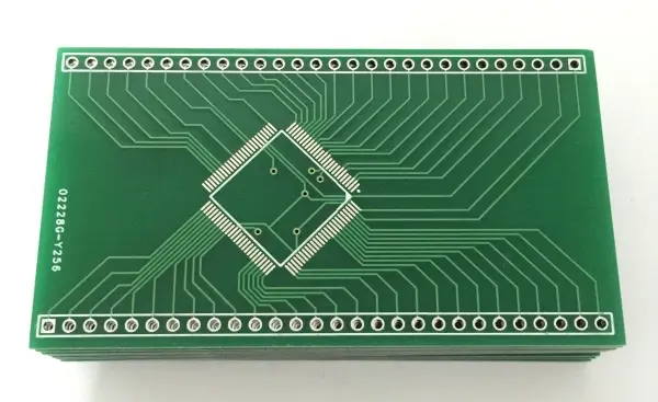
Držite ploču prema svjetlu. Ako je unutrašnja jezgra potpuno neprozirna i ne možete vidjeti svjetlo kroz unutrašnje slojeve, radi se o višeslojnoj ploči. Ako vidite samo jedan sloj bakra, radi se o jednostranoj ploči.
Pogledajte rupe. Jednostrane ploče imaju nekapljene rupe. One nemaju oblogu na zidovima rupa i izostavljaju proces elektrokapljanja. Dvostrane ploče imaju kapljene prolazne rupe ili vias. To znači da ćete vidjeti bakar unutar rupe.
Osnovna razlika je u broju bakrenih slojeva: jednostruki ima jedan bakreni sloj, dvostruki ima dva bakrena sloja, a višeslojni ima tri ili više slojeva. Kod izrade višeslojnog, dodaju se unutrašnji slojevi, a zatim se slojevi laminiraju. Možete napraviti poprečni presjek kako biste, ako je potrebno, provjerili slojeve.
Kako smanjiti EMI na jednostranim ili dvostranim tiskanim pločicama
Iz ekonomskih razloga, mnogi potrošački uređaji koriste jednostrane ili dvostrane tiskane ploče. Kako digitalna pulsna kola postaju uobičajena, problemi EMI-ja rastu. Glavni uzrok je velika površina petlje signala. Velike površine petlje ne samo da emituju jače zračenje, već i čine kolu osjetljivijom na vanjsku buku. Da bi se poboljšao EMC, najjednostavniji pristup je smanjenje površine petlje kritičnih signala.
Identificirajte ključne signale
Iz ugla elektromagnetskog smetanja (EMC), ključni signali uključuju one koji stvaraju snažno zračenje i one koji su osjetljivi na vanjsku buku. Snažni zračioci su često periodični signali, poput taktnih signala i adresnih linija niskog reda. Osjetljivi signali su često analogne linije niskog napona.
Metode za smanjenje površine petlje
Jednostavna metoda je provesti uzemljenski trag pored signalnog traga. Postavite uzemljenje što bliže. Takav raspored stvara vrlo malu petlju i smanjuje diferencijalno zračenje i osjetljivost. Kada dodate uzemljenski trag pored signala, signalna struja će uglavnom teći kroz tu malu petlju, a ne kroz druge puteve uzemljenja.
Ako koristite dvostranu ploču, postavite uzemljenje na drugu stranu, tačno ispod signalne linije. Ako možete, učinite taj vod uzemljenja širokim. Površina petlje tada je jednaka debljini ploče pomnoženoj s dužinom signalne linije. Ta površina je znatno manja od duge otvorene petlje i pomaže u smanjenju zračenja.
Također, uvijek koristite bakrenu uzemljensku mrežu na dvostranim pločama. Uzemljenska mreža smanjuje impedanciju uzemljenja. Uz uzemljensku mrežu, signalna linija gotovo uvijek ima uzemljensku liniju u blizini i formira manju petlju. Prilikom rasporeda tragova držite ključne linije blizu uzemljenja. Samo najkritičnije linije trebaju uzemljenje odmah pored sebe.
Ostali osnovni savjeti:
Koristite kratke tragove za visokobrzinske signale.
Koristite odgovarajuće kondenzatore za odvođenje blizu pinova za napajanje.
Držite analogno i digitalno uzemljenje odvojeno, a zatim ih po potrebi spojite na jednu tačku.
Izbjegavajte duge petlje. Prođite povratne staze blizu signalnog puta.
Mali praktični primjeri
Za satni trag na dvostranoj ploči, postavite široki maseni trag ispod njega na drugoj strani. Ako je debljina ploče 1,6 mm, a satni trag dugačak 50 mm, površina petlje je otprilike 1,6 mm × 50 mm. Ako trag možete skratiti na 20 mm, površina se znatno smanjuje.
Za osjetljivi analogni signal provucite uzemljenje odmah pored njega na istoj strani. Tako par formira zatvorenu petlju i smanjuje prijem smetnji.
Sažetak
Jednostrane tiskane pločice su jednostavne i jeftine. Na jednu stranu postavljaju sve komponente, a na drugu sve tragove. Dvostrane ploče dodaju drugi sloj i koriste vias za povezivanje obje strane. FR4 je uobičajeni materijal za obje. Prelazak s komponenti s provrta na površinske komponente potaknuo je potrebu za dvostranim i višeslojnim pločama. Ipak, jednostrane ploče i dalje imaju smisla za mnoge jednostavne proizvode zbog troškova i jednostavnosti. Da biste smanjili EMI na jednostranim ili dvostranim pločama, smanjite površinu petlje, dodajte obližnje uzemljene tragove, koristite mrežu uzemljenja i držite tragove kratkima.