
Single-Sided PCB Manufacturing
FLJ manufactures custom single-sided PCBs for control circuits, interfaces, lighting and other electronics that fit one copper routing layer. Our service covers FR4 bare-board fabrication, from prototypes to production, with solderable finishes and the option to continue into component assembly.
FR4 fabrication · Prototype & production · Optional assembly
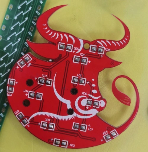
Single-Sided Boards for Everyday Electronics
A single-sided PCB, also called a single-layer PCB, carries its copper circuit on one face of an insulating substrate. Copper traces connect the pads, while the substrate supports the components and keeps separate conductors electrically isolated. It is a straightforward construction for a circuit that does not need a second routing surface.
One patterned copper face can provide the complete connection network for a low-density circuit. It combines those connections with the shape and mounting features needed in the product, while avoiding the inner-layer processing and bonding of a multilayer construction. A simple board can serve a small standalone device or one control function inside a much larger machine.
Controls and Relays
Switch inputs, relay connections and simple control functions often leave room for clear, direct routing. A single-sided board can bring those connections together with the mounting and connector positions needed by the product.
Interfaces and Household Electronics
Buttons, indicators, basic sensor interfaces and appliance controls can use a single copper pattern where their connection density permits. The board layout follows the actual circuit and housing, rather than an assumed standard rectangle.
Lighting and Power Circuits
Single-layer constructions also serve selected LED and power circuits. Copper geometry, electrical spacing and the heat path determine the useful design. A thermally demanding LED board may use a metal-based construction, covered separately on our aluminum and metal-core PCB pages.
One Routing Layer, Practical Connection Choices
Making Room for a Crossover
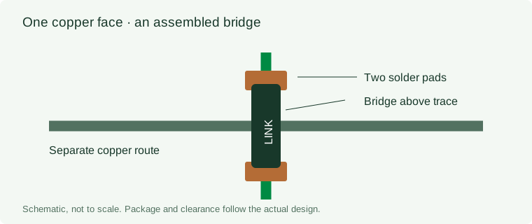
Connections that share one copper face cannot pass through each other without joining electrically. Component placement and route order resolve many crossings. Where a direct route remains blocked, a jumper can carry one connection across another.
A formed wire jumper can bridge two lead holes. A suitable zero-ohm surface-mount link can bridge between pads, allowing a separate trace beneath its body where the footprint and clearances permit. It adds a connection above the board rather than creating a second etched copper layer.
For example, a connector-to-component connection may need to cross a separate trace. A suitable link joins pads on either side of that trace, with clearance between the link and the copper beneath it. The board still has one patterned copper layer. This is an illustrative routing choice, not a required feature on every single-sided board.
The bridge is an assembly item. Its package, pad arrangement and current rating belong with the circuit and the assembly information. FLJ can supply the bare board or include jumper placement with the wider PCB assembly service.
Copper Side and Component Side
Single-sided describes the copper construction. A through-hole component can sit on the unpatterned face, with its leads passing through to solder pads on the copper face. A surface-mount component connects directly to pads on that copper face. Both arrangements use the same copper layer.
In a conventional non-plated lead hole, the lead passes through the laminate and meets the annular copper pad on the soldering face. Solder joins the lead to that exposed pad; there is no plated barrel providing an electrical connection through the board thickness. The finished opening must accept the lead, while the pad retains copper for the joint. Lead dimensions, hole dimensions and their tolerances determine that fit.
Manufacturing the Single Copper Circuit
Form the Copper Pattern
Fabrication starts with copper-clad laminate. Imaging defines the conductors, and etching removes the unwanted copper. The remaining pattern forms the traces, solder pads and copper areas required by the circuit. This one-copper route does not need inner-layer alignment or multilayer lamination.
Create the Holes and Board Shape
Drilling creates component and mounting holes. Routing forms the outline and any specified internal slots. A slot’s width and end shape follow the cutter that produces it, while its position connects the board with the parts that fit around it.
A component hole brings a lead to its copper-side pad. A mounting hole locates a fastener, while a routed opening provides clearance for a part or housing feature. Conventional single-copper lead holes can remain non-plated; a specified metallized feature follows its own manufacturing route.
Finish and Verify the Board
The board receives the specified solder mask, legend and surface finish. Open pads remain accessible for soldering, and the finished outline provides the mechanical form needed for assembly.
Copper-pattern inspection and bare-board electrical testing check the manufactured connections and isolation. Dimensional checks address the outline and relevant holes. These checks verify the fabricated board; later assembly inspection and powered testing address the populated circuit.
When One Layer Is the Better Choice
Single-sided construction offers lower manufacturing complexity when the circuit fits comfortably on one copper surface. It is particularly useful when the layout has room for direct paths and the product does not benefit from an additional routing layer.
| Design question | Single-sided direction | Reason to consider double-sided |
|---|---|---|
| Can the connections fit? | Direct routing, with limited bridges | Frequent crossovers or congested routes |
| How much board area is available? | Space for the circuit and its connections | A tighter outline that needs routing on both faces |
| What will assembly add? | A suitable component mix and manageable jumper placement | Enough added bridges to complicate the build |
| How is the full build priced? | Material, fabrication and assembly assessed together | A second layer may offset a larger board or extra assembly work |
A lower bare-board price does not necessarily mean a lower assembled-product cost. Board area, panel use, copper and finish, jumper count and placement all contribute. Comparing the complete configurations gives a more useful choice than comparing layer count alone.
A board with clear one-face routing and a small number of practical bridges can retain the simpler copper construction. If that same circuit needs a larger outline or many extra assembly operations, a double-sided layout may be the better complete build. Our double-sided PCB service covers that second routing surface and its interconnections.