


Mạch in đa lớp là gì?
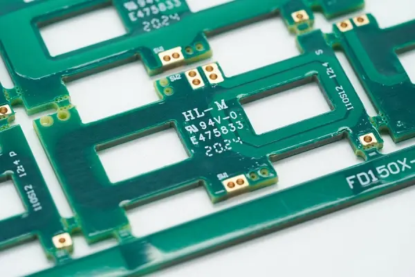
Mạch in đa lớp (Multilayer PCB) là một loại mạch in được sử dụng trong các sản phẩm điện tử, có hơn một lớp dây dẫn. Mạch in đa lớp sử dụng thêm một lớp hoặc các bảng mạch hai lớp được xếp chồng lên nhau. Ví dụ, một bảng mạch sử dụng một bảng mạch hai mặt làm lớp trong và hai bảng mạch một mặt làm lớp ngoài, hoặc hai bảng mạch hai mặt làm lớp trong và hai bảng mạch một mặt làm lớp ngoài, sẽ trở thành bảng mạch in bốn lớp hoặc sáu lớp. Các bảng mạch này được sản xuất bằng cách xếp chồng và gắn kết bằng vật liệu cách điện và sử dụng hệ thống định vị. Các mẫu dẫn điện được kết nối theo yêu cầu thiết kế. Các bảng mạch này cũng được gọi là bảng mạch in nhiều lớp.
Thiết kế mạch in nhiều lớp (PCB): Cách xác định số lượng lớp
Hiệu suất và chi phí của một bảng mạch in (PCB) phụ thuộc rất nhiều vào số lượng lớp của nó. Do đó, việc lựa chọn số lượng lớp phù hợp là rất quan trọng. Bài viết này tập trung vào các điểm chính cần xem xét khi thiết kế PCB từ 1 đến 20 lớp.
Các yếu tố quan trọng cần xem xét khi lựa chọn 1–20 lớp
Hãy bắt đầu với những điều cần xem xét. Có thể bạn đã biết sơ bộ số lớp mà PCB của bạn cần. Tuy nhiên, bạn nên tìm hiểu lý do tại sao PCB nhiều lớp có thể tốt hơn PCB một lớp. Hãy xem các điểm dưới đây để giải đáp thắc mắc của bạn:
Sử dụng hoặc ứng dụng: PCB sẽ được sử dụng ở đâu? Như đã đề cập ở trên, PCB được sử dụng trong nhiều loại thiết bị điện tử đơn giản và phức tạp. Vì vậy, bạn cần xác định xem ứng dụng của mình cần chức năng đơn giản hay phức tạp. Một thiết bị đơn giản có thể hoạt động tốt với một lớp. Một thiết bị phức tạp thường cần nhiều lớp hơn.
Loại tín hiệu cần thiết: Các bảng mạch có cần truyền tín hiệu vi sóng hoặc tần số cao không? Lựa chọn lớp mạch cũng phụ thuộc vào loại tín hiệu mà chúng phải truyền. Tín hiệu có thể là tần số cao, tần số thấp, tín hiệu đất hoặc tín hiệu nguồn. Nếu ứng dụng của bạn cần nhiều đường dẫn tín hiệu khác nhau hoặc tín hiệu hỗn hợp, bạn sẽ cần một bảng mạch in nhiều lớp (PCB). Các mạch này cũng có thể cần các lớp đất và lớp chắn riêng biệt.
Qua các loạiLoại lỗ vias bạn chọn là một yếu tố quan trọng khác. Nếu bạn chọn lỗ vias chôn ngầm hoặc lỗ vias mù, bạn có thể cần thêm các lớp bên trong. Do đó, việc lựa chọn lỗ vias có thể ảnh hưởng đến số lượng lớp cần thiết.
Độ dày và số lượng lớp tín hiệu cần thiếtQuyết định về số lớp cũng phụ thuộc vào hai yếu tố quan trọng: lớp tín hiệu và mật độ chân. Số lượng lớp trên PCB có xu hướng tăng khi mật độ chân tăng. Ví dụ, nếu mật độ chân là 1.0, bạn có thể cần 2 lớp tín hiệu. Nhưng nếu mật độ chân nhỏ hơn 0.2, bạn có thể cần 10 lớp hoặc hơn.
Số lượng máy bay cần thiếtCác lớp nguồn và lớp đất giúp giảm nhiễu điện từ (EMI) và bảo vệ các lớp tín hiệu. Do đó, số lượng lớp bạn cần sẽ ảnh hưởng đến việc lựa chọn lớp. Nhiều lớp hơn có nghĩa là nhiều lớp hơn.
Chi phí sản xuấtMặc dù chi phí không phải là yếu tố duy nhất, nhưng nó là một yếu tố quan trọng trong việc lựa chọn số lớp cho thiết kế PCB từ 1 đến 20 lớp. Chi phí sản xuất PCB tăng lên khi số lớp tăng. PCB nhiều lớp đắt hơn so với PCB một lớp. Chi phí sẽ phụ thuộc rất nhiều vào các yêu cầu được liệt kê ở trên.
Thời gian giao hàngThời gian giao hàng cho đơn hàng PCB từ 1–20 lớp phụ thuộc vào tất cả các yếu tố nêu trên. Ví dụ, nếu thiết kế của bạn chỉ cần một lớp, thời gian giao hàng có thể ngắn. Nếu bạn đặt hàng bảng mạch cho các thiết bị điện tử công nghiệp phức tạp, thời gian giao hàng sẽ lâu hơn.
Nếu bạn không thể quyết định dựa trên các điểm trên, bạn có thể thảo luận về nhu cầu của mình với nhà sản xuất PCB Philifast.
Những ưu điểm và nhược điểm của mạch in đa lớp (PCB) là gì?
So với bảng mạch in một mặt (PCB), bảng mạch in nhiều lớp (PCB) có những khác biệt rõ rệt về bề mặt và hiệu suất hoạt động. Những khác biệt này là yếu tố quan trọng quyết định độ bền và chức năng của bảng mạch. Các ưu điểm chính của PCB nhiều lớp bao gồm khả năng chống oxy hóa, cấu trúc đa dạng, mật độ cao và việc sử dụng các kỹ thuật phủ bề mặt để đảm bảo chất lượng và an toàn của bảng mạch. Dưới đây là các tính năng quan trọng về độ tin cậy cao và ưu nhược điểm của PCB nhiều lớp:
1. Độ dày lớp đồng trên thành lỗ thông thường là 25 micron.
Lợi thế: Độ tin cậy cao hơn, bao gồm khả năng chống giãn nở theo trục z tốt hơn. Lớp đồng dày hơn trên thành lỗ giúp tăng độ bền và tuổi thọ.
Rủi roCó một số rủi ro. Trong quá trình sử dụng thực tế, các vấn đề như nổ vỡ hoặc thoát khí, hoặc các vấn đề trong quá trình lắp ráp, có thể ảnh hưởng đến các kết nối điện. Những vấn đề này có thể gây ra sự tách lớp bên trong hoặc nứt thành lỗ. Dưới tải trọng, các lỗi này có thể dẫn đến hỏng hóc. IPC Class 2 (tiêu chuẩn được áp dụng cho nhiều nhà máy) có thể yêu cầu lớp mạ đồng trên bảng mạch đa lớp phải nhỏ hơn 20% [lưu ý: câu này giữ nguyên tham chiếu số liệu gốc].
(Lưu ý: Chi tiết cụ thể của quy tắc IPC phụ thuộc vào bộ quy tắc và quy trình sản xuất của nhà máy. Điểm quan trọng ở đây là việc mạ lỗ và kiểm soát quá trình này ảnh hưởng đến độ tin cậy.)
2. Không sửa chữa bằng hàn hoặc sửa chữa mạch hở.
Lợi thếMột mạch hoàn hảo giúp tăng cường độ tin cậy và an toàn. Không cần bảo trì trong quá trình sử dụng bình thường.
Rủi roNếu việc sửa chữa không đạt yêu cầu, mạch in đa lớp (PCB) có thể bị hở mạch. Ngay cả khi được sửa chữa đúng cách, trong điều kiện tải như rung động, vẫn có thể có nguy cơ hỏng hóc. Điều này có thể dẫn đến sự cố trong quá trình sử dụng.
3. Tiêu chuẩn vệ sinh vượt quá tiêu chuẩn IPC.
Lợi thếĐộ sạch cao hơn trên bảng mạch in nhiều lớp (PCB) giúp tăng độ tin cậy.
Rủi roCác tạp chất trên bảng mạch và sự tích tụ của hàn có thể gây hại cho lớp phủ hàn. Các tạp chất ion có thể gây ăn mòn và ô nhiễm trên bề mặt hàn. Điều này có thể dẫn đến các vấn đề về độ tin cậy như mối hàn kém hoặc lỗi điện và, cuối cùng, tăng nguy cơ hỏng hóc thực tế.
4. Kiểm soát nghiêm ngặt thời hạn sử dụng cho từng loại bề mặt hoàn thiện.
Lợi thếKiểm soát tốt bề mặt giúp hàn tốt hơn, tăng độ tin cậy và giảm nguy cơ thấm ẩm.
Rủi ro: Các lớp hoàn thiện bề mặt cũ trên các bảng mạch đa lớp cũ có thể xuất hiện các thay đổi về mặt kim loại. Điều này có thể gây ra vấn đề về khả năng hàn. Sự xâm nhập của độ ẩm có thể gây ra vấn đề trong quá trình lắp ráp hoặc bong tróc sau này trong quá trình sử dụng. Điều này có thể dẫn đến sự tách rời của các lớp bên trong và mạch hở.
Dù là trong quá trình sản xuất và lắp ráp hay trong quá trình sử dụng thực tế, các bảng mạch in nhiều lớp (PCB) phải đảm bảo hiệu suất đáng tin cậy. Tất nhiên, độ tin cậy này phụ thuộc mạnh mẽ vào trình độ kỹ thuật và quy trình sản xuất của nhà sản xuất.
Sự khác biệt giữa việc tạo mẫu PCB một lớp và nhiều lớp
Khi thiết kế và sản xuất bảng mạch in (PCB), bạn cần quyết định xem loại PCB một lớp hay nhiều lớp phù hợp với thiết bị của mình. Cả hai loại đều được sử dụng trong nhiều ứng dụng tiêu chuẩn. Tuy nhiên, loại PCB cần thiết phụ thuộc vào mục đích sử dụng của bảng mạch. Mỗi loại có những đặc điểm riêng biệt giúp nó phù hợp với các tác vụ cụ thể. Các thiết bị gia dụng đơn giản thường sử dụng bảng mạch một lớp. Các máy móc phức tạp hơn cần thiết kế PCB nhiều lớp.
Bo mạch in một lớp
Một lớp hoặc Bảng một mặt bao gồm một lớp nền, một lớp kim loại dẫn điện và một lớp phủ hàn bảo vệ và in mực. Hầu hết các quy trình sản xuất sử dụng đồng làm kim loại dẫn điện. Một mặt của bảng mạch chứa tất cả các linh kiện cần thiết. Mặt còn lại có mẫu dẫn điện.
Vì thiết kế của chúng đơn giản hơn so với bảng mạch hai mặt và nhiều lớp, bảng mạch in một lớp (single-layer PCBs) có chi phí thấp hơn và dễ sản xuất hơn. Thiết kế đơn giản này cũng là nhược điểm chính của chúng. Chúng có ít điểm kết nối hơn. Do đó, bảng mạch in một lớp có tốc độ thấp hơn và ít lựa chọn hơn trong việc bố trí mạch phức tạp.
Bo mạch in hai mặt
Một lựa chọn khác là bảng mạch in hai mặt (double-sided PCB). Nó có nhiều lớp hơn bảng mạch in một mặt, nhưng ít hơn bảng mạch in nhiều lớp. Giống như loại một mặt, bảng mạch in hai mặt sử dụng một lớp nền. Sự khác biệt chính là bảng mạch in hai mặt có lớp kim loại dẫn điện ở cả hai mặt của lớp nền.
Bo mạch hai mặt cho phép truyền dẫn nhiều tín hiệu hơn so với bo mạch một mặt. Chúng vẫn có giá thành thấp hơn so với bo mạch nhiều lớp. Đây là lựa chọn phù hợp cho nhiều thiết kế.
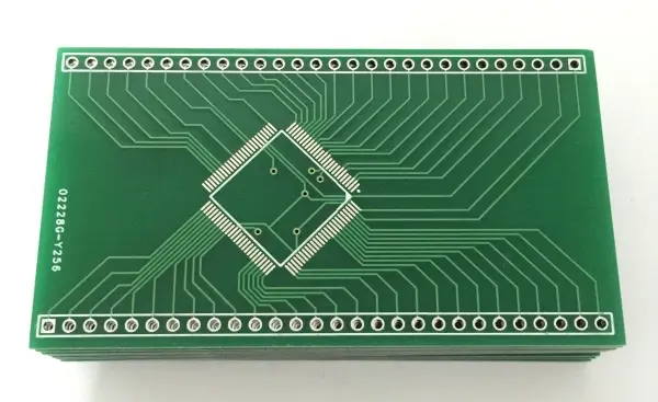
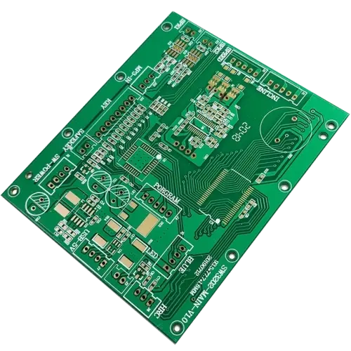
Bo mạch in nhiều lớp
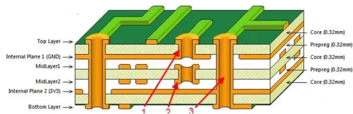
Một bảng mạch in đa lớp (PCB) bao gồm ba hoặc nhiều bảng mạch hai mặt được gắn kết với nhau bằng keo đặc biệt. Mỗi bảng mạch có vật liệu cách điện giữa các lớp. Mặc dù bảng mạch đa lớp có thể sử dụng nhiều bảng mạch xếp chồng lên nhau, hầu hết đều có số lớp chẵn, thường từ 4 đến 12. Điều này là do số lớp lẻ có thể gây cong vênh và xoắn sau khi hàn.
Với nhiều lớp và nhiều kết nối hơn, bảng mạch in đa lớp (PCB) phù hợp với các thiết bị cần nhiều chức năng và tính năng tiên tiến. Chúng có khả năng hoạt động cao hơn và hiệu suất tín hiệu nhanh hơn so với bảng mạch in một mặt hoặc hai mặt. Tuy nhiên, thiết kế của chúng phức tạp hơn, chi phí cao hơn, thời gian sản xuất lâu hơn và cần được bảo dưỡng và lắp ráp cẩn thận hơn.
Ghi chú cuối cùng
Lựa chọn loại PCB phù hợp phụ thuộc vào nhu cầu sản phẩm, loại tín hiệu, mật độ chân cắm, yêu cầu về lớp mặt phẳng, giới hạn chi phí và thời gian giao hàng. Nếu bạn không chắc chắn, hãy thảo luận với nhà sản xuất sớm. Một nhà sản xuất PCB uy tín có thể giúp bạn cân nhắc giữa chi phí, hiệu suất và thời gian giao hàng. Nếu bạn cần hỗ trợ về số lớp và cấu trúc lớp cho một sản phẩm cụ thể, bạn có thể thảo luận thiết kế với Philifast hoặc một nhà sản xuất PCB có kinh nghiệm khác.
Câu hỏi thường gặp
Chúng cho phép tăng mật độ mạch, cải thiện tính toàn vẹn tín hiệu, giảm kích thước/trọng lượng bo mạch, phân phối nguồn điện tốt hơn (với các lớp nội bộ) và khả năng định tuyến phức tạp hơn so với bo mạch in một mặt hoặc hai mặt.
Bo mạch đa lớp thông thường có 4, 6, 8, 10 hoặc nhiều lớp hơn. Số lượng lớp phụ thuộc vào độ phức tạp của linh kiện, đường dẫn tín hiệu, yêu cầu về lớp nguồn và lớp đất, kiểm soát trở kháng, quản lý nhiệt và chi phí.
Vật liệu cách điện (prepregs và vật liệu lõi) thường là sợi thủy tinh epoxy FR-4, vật liệu laminate tốc độ cao hoặc vật liệu chuyên dụng có độ suy hao thấp cho ứng dụng RF/microwave; sự lựa chọn này ảnh hưởng đến độ bền của bảng mạch, hằng số điện môi (Dk), hệ số giãn nở nhiệt (CTE) và hiệu suất tổng thể.
Các loại bề mặt hoàn thiện phổ biến bao gồm HASL (không chứa chì hoặc chứa chì), ENIG, bạc/thiếc ngâm, OSP và các loại đặc biệt hơn dành cho yêu cầu độ tin cậy cao hoặc điều kiện môi trường cụ thể. Lựa chọn bề mặt hoàn thiện ảnh hưởng đến khả năng hàn, tuổi thọ lưu trữ và hiệu suất tiếp xúc.
Cung cấp đầy đủ các lớp Gerber/Drill/NC, sơ đồ xếp lớp rõ ràng kèm theo giá trị điện môi/hằng số điện môi, trọng lượng đồng, độ dày bảng mạch hoàn thiện, yêu cầu về lỗ via/lỗ via ẩn/lỗ via chôn, lớp phủ bề mặt, lớp phủ hàn/lớp in, và số lượng. Yêu cầu báo cáo DFM.