
Multilayer PCB Manufacturing
FLJ manufactures custom multilayer PCBs for prototypes and production. Combine internal routing, power and ground layers in a board built around your circuit, with material, copper and interconnection options for the finished product.
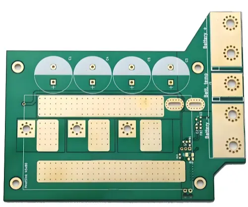
Routing space.
Reference layers.
One laminated board.
Choose the copper arrangement, dielectric buildup and connections as one construction.
Compare multilayer options ↓Multilayer PCB Options for Your Design
More copper layers give a circuit additional routing space and room for reference planes. A multilayer PCB combines more than two conductive layers with insulating material between them. The layer count is the number of copper layers, not the number of components or mounting faces.
Configure the complete board
| Choice | Available construction | What it changes |
|---|---|---|
| Material | FR-4, high-Tg and suitable specialty constructions | Electrical loss, thermal behavior and the lamination system |
| Thickness | Custom finished thickness and dielectric buildup | Mechanical fit and spacing between copper layers |
| Copper | Separately specified inner and finished outer copper | Conductor geometry, current paths and the surrounding buildup |
| Finish and delivery | ENIG, HASL, OSP; individual boards or panels | Exposed-pad finish and the format for subsequent assembly |
Changing the copper weight or a material can also change the dielectric buildup needed for the same finished thickness. A quotation therefore covers the construction, rather than the copper-layer count alone.
A Stackup Built Around Your Circuit
A stackup describes the order and construction of the board’s copper and dielectric layers. Two boards with the same layer count and overall thickness can have different distances between a signal layer and its reference plane.
Copper, core and prepreg
In a common rigid multilayer construction, circuits are formed on the copper faces of cured cores. Those copper faces become internal layers. Prepreg supplies reinforcing glass fabric and partially cured resin between the cores and outer copper foil. During lamination, its resin flows around the etched copper features and cures, forming a bonded insulating layer.
The six-copper-layer illustration shows two internal cores joined with prepreg and outer foil. It identifies the physical materials separately from the electrical roles assigned to the copper. It is a construction example, not a dimensioned FLJ standard stackup.
The dielectric is part of the circuit’s geometry. Its material properties and pressed thickness work with the trace dimensions to determine characteristic impedance. Resin filling around copper changes the buildup, so the prepreg’s starting specification alone does not define the final dielectric spacing.
Inner copper is patterned from the core’s cladding, while outer copper can gain thickness during plating. Specifying inner copper and finished outer copper separately keeps the stackup tied to the conductors that will actually be manufactured.
Place the signal beside its reference
A reference plane gives a nearby signal a return-current path. Its continuity and distance from the trace matter. A split or interruption in the reference can force the return current to take a different route even when the board has many layers.
We build the stackup to support the intended arrangement of routing and planes, the required finished thickness and any controlled-impedance geometry. Layer count makes those arrangements possible; it does not replace them.
Material properties and selection →Building the Internal Circuit
The internal circuit is manufactured before it is enclosed in the finished laminate. Its copper pattern, location and connection to the drilled holes must all fit the same board design.
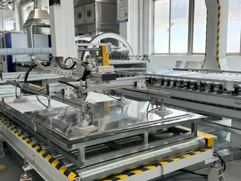
Pattern the copper.
Align the layers.
Bond the stack.
Form and inspect the inner copper
Imaging and etching define the internal traces, pads, planes and clearances on the core. Inner-layer AOI compares the visible copper pattern with the fabrication data to find pattern defects before the surfaces become inaccessible. Inspecting at this stage gives direct access to the inner artwork.
Align and laminate the stack
The inner cores, prepreg and outer copper are brought together in the required sequence. Registration aligns the inner patterns so a later drilled hole meets its intended inner pads, with clearances around copper belonging to other nets. Surface preparation promotes bonding at the internal interfaces.
Heat and pressure allow the prepreg resin to flow, fill around the copper pattern and cure. The result is a bonded laminate with the intended separation between conductors. Resin content, copper distribution and the selected material system all affect this construction; lamination is more than adding the starting sheet thicknesses together.
Create the connections and outer circuit
In a conventional through-hole multilayer build, drilling follows lamination. Hole preparation and copper metallization establish the connection between the outer faces and the intended inner-layer pads. Copper clearances isolate the hole from layers that must not join that net. Outer-layer imaging, plating and etching then complete the surface circuit through the selected fabrication route.
Blind and buried connections can require a different buildup sequence. These constructions are planned with the relevant subassemblies and interconnection stages, rather than added to a finished through-hole board.
Interconnections That Match the Stack
The useful via is the one that reaches the required layers while preserving space for other connections. Different via spans also create different fabrication routes.
Through-hole vias
A plated hole passes through the board. It can connect to designated copper pads on intermediate layers as well as the outside faces. The barrel’s full depth does not mean every plane it crosses is electrically connected to it.
Blind vias
A blind via connects an outer copper layer to a selected inner layer without passing through the whole board. It can free routing area elsewhere, with its depth and formation method matched to the construction.
Buried vias
A buried via connects internal layers and is enclosed when the remaining stack is laminated. Its position in the buildup determines when the internal connection must be made and checked.
Span illustrations only. Pads, hole clearances and manufacturing dimensions are omitted.
FLJ manufactures conventional through-hole multilayers as well as constructions requiring blind, buried or HDI interconnections. An internal connection made in a subassembly adds processing before the complete board is laminated. That buildup route, the material system and drilling geometry influence cost alongside the number of copper layers. The dedicated HDI service covers microvia and buildup choices in greater detail.
HDI PCB manufacturing →Checking What Is Inside the Board
A finished surface cannot show every feature of a multilayer board. Inspection and testing address the internal artwork, the laminated geometry and the electrical network at different stages.
| Object | Stage or method | Information obtained |
|---|---|---|
| Internal copper pattern | Inner-layer AOI before lamination | Visible pattern defects such as missing copper, bridges or unwanted copper |
| Layer and drill relationship | Registration and drilling checks | Alignment of the layers and hole positions against the intended geometry |
| Dielectric and plated section | Microsection where the construction calls for it | A local view of layer separation, interfaces and hole-wall copper |
| Required electrical network | Bare-board electrical testing | Opens and unintended connections against the fabrication net data |
| Controlled-impedance construction | Impedance measurement of the specified test structure or coupon | Whether the representative geometry meets its impedance target |
A microsection reveals a local cut through the laminated specimen; the network test checks the required connections and isolation across the bare board. An impedance coupon represents the specified trace construction rather than testing every production signal trace. Together, the applicable checks address different features of the multilayer build. FLJ also provides PCB assembly and populated-board testing when the order continues beyond bare-board fabrication.
Related multilayer PCB designs
Explore the board images, product information and design details for related projects.
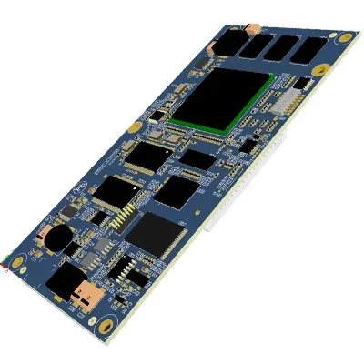
10-Layer Communication Switch PCB and PCBA Design
A ten-layer PCB and PCBA design profile for a communication switch.
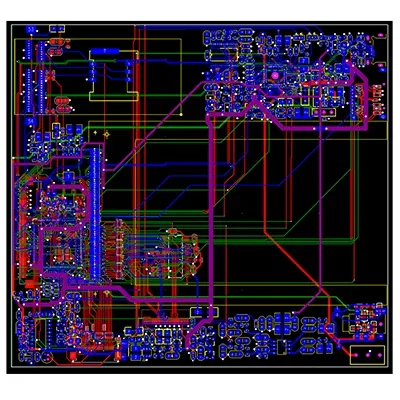
8-Layer Communication PCB and PCBA Design
An eight-layer PCB and PCBA design profile for communication electronics.
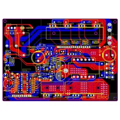
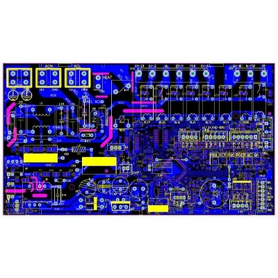
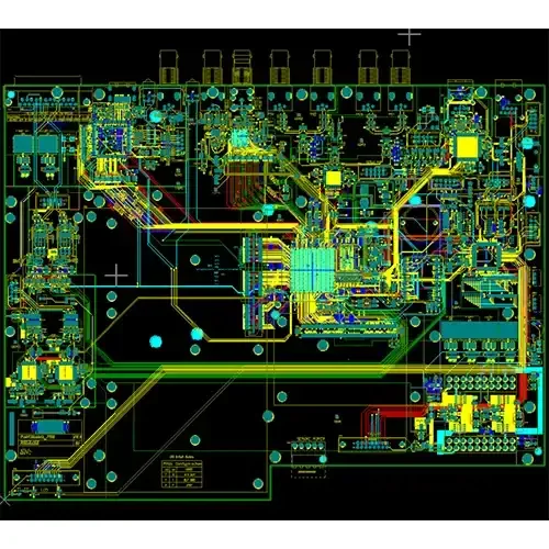
4-Layer Medical Equipment PCB and PCBA Design
A four-layer PCB and PCBA design profile for medical equipment.
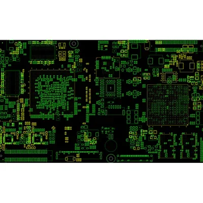
6-Layer Core Module PCB Design
A six-layer core-module PCB design with length-matched signal groups and a controlled-impedance fabrication profile.
12-Layer Automotive High-Speed Backplane Design
A twelve-layer high-speed backplane design for automotive electronics.