1. لمحة عامة
تُستخدم الفتحات العمياء والفتحات المدفونة بشكل أساسي للألواح عالية الكثافة وللألواح ذات الثقوب الصغيرة جدًا. والهدف هو توفير مساحة التوجيه وبالتالي جعل ثنائي الفينيل متعدد الكلور أصغر. ومن الأمثلة الشائعة على ذلك لوحات ثنائي الفينيل متعدد الكلور للهواتف المحمولة.
2. التصنيف
أ) الحفر بالليزر
1. أسباب استخدام الحفر بالليزر
a. يطلب العميل الحفر بالليزر.
b. يمكن أن تكون الشقوق العمياء صغيرة جدًا (<= 6 ميل)، لذا فإن الليزر فقط هو الذي يمكنه حفرها بشكل موثوق.
c. بالنسبة للمداخن الخاصة العمياء والمدفونة - على سبيل المثال، إذا كان هناك ممر أعمى من L1 إلى L2 وممر مدفون من L2 إلى L3 - يلزم إجراء حفر بالليزر.
2. مبدأ الحفر بالليزر
يستخدم الحفر بالليزر الحرارة الصادرة من الليزر لتبخير أو إذابة مادة اللوح وإحداث ثقب. ولكي ينجح ذلك، يجب أن تمتص مادة اللوح طاقة الليزر. ولهذا السبب، يشيع استخدام المواد من نوع RCC لأنها لا تحتوي على قماش من الألياف الزجاجية وبالتالي لا تعكس الليزر.
3. مقدمة موجزة عن مادة RCC
RCC تعني النحاس المطلي بالراتنج. وهو عبارة عن رقائق نحاس تحتوي على طبقة من الراتنج الخاص على الجانب الخشن من رقائق النحاس الإلكتروليتي.
لدينا في شركتنا ثلاثة موردين لـ RCC: Shengyi وMitsui وLG.
خيارات المواد: سمك الراتنج 50، 65، 70، 75، 80 ميكرومتر، وسمك رقائق النحاس 12، 18 ميكرومتر، إلخ.
يأتي RCC في درجات Tg العالية و Tg المنخفضة. وعادةً ما يكون ثابت العزل الكهربائي أقل من FR-4 القياسي. على سبيل المثال، يتميز S6018 من Shengyi بثابت عازل كهربائي يبلغ 3.8، لذا توخ الحذر عندما تحتاج إلى التحكم في المعاوقة.
للحصول على تفاصيل حول مواد معينة، يرجى سؤال فريق هندسة المنتجات أو فريق البحث والتطوير.
4. متطلبات الأدوات والأدوات اللازمة للحفر بالليزر
أ) من الصعب أن يحرق الليزر النحاس. لذا قبل الحفر بالليزر، احفر خلوصًا نحاسيًا في مواضع الثقب الأعمى. يجب أن يتطابق الخلوص مع حجم الثقب النهائي.
ب) تضاف علامات تحديد المواقع للحفر بالليزر على الطبقة L2/ L(N-1). ضع علامة على ذلك في صفحة تغيير طبقة MI.
C) يجب أن يكون الفيلم الخاص بنقش البقع العمياء عبر البقع من إنتاج LDI. يجب أن تستخدم الألواح المقطوعة والأدوات المقطوعة حجم لوحة LDI.
5. ميزات تدفق الإنتاج
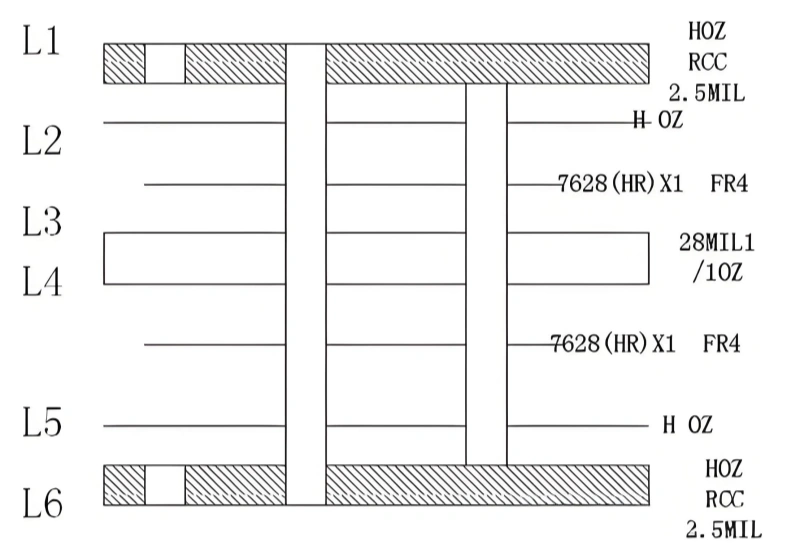
أ) عندما يكون العدد الإجمالي لطبقات اللوحة N، قم بإعداد طبقات L2-L(N-1) أولاً باتباع عملية الطبقات الداخلية العادية.
ب) بعد التصفيح وبعد توجيه مخطط اللوحة، قم بتغيير التدفق على النحو التالي:
→ حفر ثقوب تسجيل LDI ← حفر ثقوب تسجيل LDI ← غشاء جاف ← حفر بقع عمياء عبر القنوات ← حفر بالليزر ← حفر عبر الثقوب ← نحاس غير مكهرب ← (عملية عادية).
6. ملاحظات أخرى
أ) مواد RCC غير معتمدة من UL في كثير من الحالات. لذا لا تضيف علامة UL إلى هذه الألواح في الوقت الحالي.
ب) حول تخطيط اللوحة و MI: لتجنب التعامل مع المخططات التي تتضمن RCC على أنها ألواح ذات طبقات مزيفة (يقوم متجر أفلام MI بتصنيع أفلام ذات طبقات مزيفة بشكل مختلف عن الأفلام العادية)، افصل RCC عن L2 أو L(N-1) عند رسم هيكل اللوحة. على سبيل المثال، انظر تخطيط اللوحة SR2711/01.
C) IPC-6016 هو معيار لوحة HDI:
- سمك النحاس الأعمى بالليزر عبر الجدار النحاسي: 0.4 مل (دقيقة).
- متطلبات شريحة اللحام: يُسمح بالتماس.
- إذا كان حجم الوسادة لا يزيد عن 5 مل أكبر من قطر الثقب، ففكر في إضافة دمعة.
د) حافظ على حافة اللوح ≥ 0.8”.
ب) الحفر الميكانيكي للفتحات العمياء/المحفورة
1. نطاق التطبيق
عندما يكون حجم لقمة الحفر ≥ 0.20 مم، ضع في اعتبارك الحفر الميكانيكي.
2. طريقة تصفيح الشقوق العمياء/المحفورة (انظر إشعار RD TSFMRD-113)
أ) في العادة، قد يحتوي السطح النحاسي لدائرة أي طبقة على خطوة طلاء لوحة واحدة فقط بالإضافة إلى خطوة طلاء نمط واحد.
ب) في العادة، بعد انتهاء عملية التصفيح الكامل وسُمك اللوح ≥ 80 ميللتر، تتطلب الثقوب العابرة طلاء اللوحة + طلاء النمط. لذلك، عند طلاء الفتحات العمياء، يجب ألا يكون سطح الطبقة الخارجية مطليًا باللوحة.
C) إذا تم استيفاء البندين أعلاه، يتم الطلاء الأعمى عبر الطلاء على النحو التالي:
I) إذا كان عرض أثر الطبقة الخارجية > 6 ميل وسُمك اللوحة عبر الفتحة < 80 ميل، فعندئذٍ أثناء الطلاء الأعمى عبر الطبقة الخارجية قد يكون سطح اللوحة الخارجية مطليًا باللوحة.
ثانيًا) إذا كان عرض أثر الطبقة الخارجية > 6 ميل ولكن سمك اللوحة عبر الفتحة > 80 ميل، فعندئذٍ يحتاج سطح الطبقة الخارجية أثناء الطلاء الأعمى عبر الممر إلى حماية غشاء.
ثالثًا) إذا كان عرض أثر الطبقة الخارجية < 6 ميل وسُمك اللوحة عبر الفتحة ≥ 80 ميل، فعندئذٍ يحتاج سطح الطبقة الخارجية أثناء الطلاء الأعمى عبر الممر إلى حماية غشاء.
3. طرق الغشاء (قناع اللحام/الغشاء الجاف)
- عندما تكون نسبة العرض إلى الارتفاع L/D ≤ 0.8، يتم وضع طبقة جافة على سطح الطبقة الخارجية وتعريض اللوحة بالكامل. ثم يتم طلاء أسطح الطبقة الداخلية العمياء عبر الطبقة الداخلية بطبقة كهربائية كلوحة كاملة.
- عندما تكون نسبة العرض إلى الارتفاع L/D > 0.8، قم بتطبيق فيلم جاف على سطح الطبقة الخارجية وتعريض البقع العمياء فقط. لهذا يجب عمل فيلم تعريض موضعي للطلاء أو استخدام تعريض LDI. ثم يتم طلاء أسطح الطبقة الداخلية العمياء ذات الممرات العمياء بالكهرباء كلوحة كاملة.
4. طرق تعريض البقع العمياء عبر البقع العمياء
- بالنسبة للفتحات العمياء ≤ 0.4 مم (16 ميل)، استخدم LDI لكشف البقع العمياء.
- بالنسبة للفتحات العمياء > 0.4 مم (16 ميل)، استخدم غشاء لكشف البقع العمياء.
5. طرق التغليف للأفياش المدفونة
- عندما يكون عرض التتبع الجانبي المدفون ≤ 4 مل، يحتاج السطح المدفون إلى غشاء لكشف البقع.
- عندما يكون عرض التتبع الجانبي المدفون في المقطع الجانبي المدفون > 4 مل، يمكن طلاء السطح المدفون في المقطع الجانبي المدفون مباشرة.
6. ملاحظات ونقاط يجب تذكرها
- بالنسبة لنسبة العرض إلى الارتفاع L/D: L = سُمك العازل الكهربائي + سُمك النحاس، D = قطر الشق الأعمى/المحفور.
- بالنسبة لأغشية الطلاء الأعمى/المحفورة عبر التصفيح: قطر بقعة التعريض D_spot = D - 6 (ميل).
- أضف علامات المحاذاة إلى فيلم بقعة التعريض. يجب أن تتطابق إحداثياتها مع الثقوب المرجعية الخارجية.
- عادةً ما يتم طلاء الشقوق العمياء التي تحتاج إلى حماية غشاء بتيار نبضي (AC) أثناء الطلاء الكهربائي.
3. المتطلبات الخاصة وملاحظات العملية الخاصة بالألواح العمياء عبر الإنترنت
- فيات عمياء مملوءة بالراتنج:
عندما تكون أحجام الفتحات المدفونة كبيرة ويوجد العديد من الثقوب، قد يحتاج ضغط اللوحة إلى الكثير من الراتنج لملء الفتحات. لتجنب تأثير ذلك على السُمك النهائي للوحة، قد تطلب شركة R&D ملء الفتحات المدفونة مسبقًا بالراتنج قبل التصفيح. يمكن أن تتبع طريقة التعبئة طريقة ملء قناع اللحام الأخضر عبر التعبئة. - عندما تحتوي الطبقة الخارجية على فيات عمياء:
a. أثناء الكبس يمكن أن يتسرب الراتنج من الطبقة الخارجية. لذا بعد التصفيح تضاف خطوة إزالة الراتنج (إزالة الصمغ).
b. قبل تجفيف الطبقة الخارجية يتم تنظيف سطح اللوح قبل تجفيف الطبقة الخارجية وهناك خطوة تلميع اللوح. يكون النحاس الكيميائي (النحاس غير المكهرب) رقيقًا جدًا (0.05-0.1 مل فقط)، لذلك قد يتآكل أثناء التلميع. لتجنب ذلك، أضف خطوة تصفيح اللوح لتكثيف النحاس. التدفق النموذجي: التصفيح ← إزالة الراتنج ← الحفر ← الحفر ← النحاس غير الكهربائي ← طلاء اللوحة ← الطلاء اللوحي ← الطلاء الجاف ← الطلاء بالنمط. - الألواح ذات الطبقات العالية العمياء عبر الألواح ذات الطبقات العالية و PIN-LAM:
عند صنع ألواح ذات طبقات عديدة وشقوق عمياء، يمكن استخدام تصفيح PIN-LAM. لاحظ أن ماكيناتنا يمكنها فقط حفر ثقوب PIN-LAM عندما يكون سمك اللب أقل من 30 ميل. في العديد من الحالات، ما زلنا نستخدم التصفيح العادي؛ على سبيل المثال PR4726010 مصنوعة من التصفيح العادي. - حافة اللوحة:
نظرًا لأنه قد يكون هناك العديد من التصفيحات والعديد من ثقوب المعالجة، اترك حافة اللوح ≥ 0.8”. - بطاقة LOT وملاحظات اللجنة:
عند كتابة بطاقة LOT، بالنسبة للعمليات الفرعية، يجب كتابة بنية اللوحة للعملية الفرعية الواحدة وكذلك كتابة بنية لوحة العملية الرئيسية في المتطلبات الخاصة. هذا يساعد العمليات اللاحقة. - مكان وضع الطبقة الجافة العمياء (الطبقة الداخلية أو الخارجية):
اذكر أمثلة: إذا كانت سماكة A للقلب أكبر من 12 ميل (باستثناء سماكة النحاس)، فضع الطبقة الجافة على الطبقة الخارجية. إذا كان سمك A للقلب أقل من 12 ميل (باستثناء سمك النحاس)، فضع الطبقة الجافة على الطبقة الداخلية.
4. التذكيرات السريعة والقيم المحددة
- حافظ على حافة اللوح ≥ 0.8 بوصة.
- ليزر أعمى عبر الجدار النحاسي ≥ 0.4 مل.
- بالنسبة لفرق حجم الوسادة مقابل حجم الفتحة ≤ 5 مل، اقترح قطرات الدموع.
- استخدم RCC للحفر بالليزر لأن RCC يمتص الليزر.
- بالنسبة للطلاء الأعمى/المحفور عبر اللوحات، تحقق من عرض أثر الطبقة الخارجية وسُمك اللوحة الكلي لتحديد ما إذا كان يجب طلاء اللوحة أو حمايتها بغشاء.
- L/D = (عازل + نحاس) / قطر الثقب. استخدم هذا لاختيار طرق التعريض والأفلام.