

















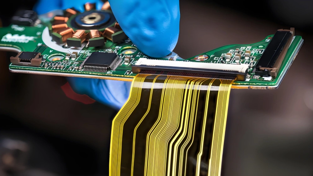
ثم تحاول بناء منتج فعلي باستخدامه. جهاز قابل للارتداء يُطوى حول بطارية. مستشعر طبي يجب أن يتحمل التعرق والمواد الكيميائية المستخدمة في التنظيف والاهتزازات، مع الحفاظ على قراءة الميكروفولت بدقة. وحدة كاميرا لا تتوفر فيها أي مساحة إضافية. وفجأة، تتحول عبارة “يمكن ثنيه” إلى قائمة من الأسئلة.
أين بالضبط أسمح بالانحناء؟
ماذا يحدث لـ مفاصل اللحام بالقرب من المنعطف?
كيف يمكنك حتى تشغيل SMT على شيء يتلوى مثل الشريط؟
هذا الدليل هو النسخة العملية. فهو يشرح ماهية تجميع اللوحات المطبوعة المرنة (التي تُكتب غالبًا بـ FPCA)، وكيف تختلف هذه العملية عن اللوحات الصلبة، وما الذي يجب الانتباه إليه عند التصميم، وكيف يبدو مسار التصنيع الفعلي، وأين تتكبد التكاليف وتقل العائدات عادةً.
ما الذي يعنيه مصطلح "تجميع لوحات الدوائر المطبوعة المرنة" في الواقع
تجميع لوحات الدوائر المطبوعة المرنة هي عملية تركيب المكونات مباشرةً على ركيزة دائرة مرنة، وعادةً ما تكون رقيقة فيلم أساسي من البوليميد (PI) بورق نحاسي. تبدو خطوات التجميع مشابهة لتلك الخاصة بلوحات الدوائر المطبوعة الصلبة (PCBA)، لكن الخصائص الفيزيائية تختلف تمامًا.
لوحة FR4 الصلبة مسطحة. وهي تظل مسطحة. كما أنها تتحمل دورات إعادة الانصهار المعتادة بشكل جيد.
الدائرة المرنة الخالصة تحتاج إلى الحركة.
كما أنه يتوسع ويتقلص بشكل أكبر. ويمتص الرطوبة. ويتجعد. وقد يرتفع أثناء التركيب. وقد يتشوه بدرجة كافية تجعل من المساحة المخصصة للمسافات الصغيرة بين المكونات مشكلةً حتى لو كان تصميم CAD مثاليًا.
إذن، فإن الموضوع الرئيسي في التجميع المرن هو تحقيق الاستقرار. فأنت تُجبر اللوحة المرنة باستمرار على التصرف كلوحة صلبة لفترة كافية لطباعة المعجون، ووضع المكونات، وإعادة الصهر، والفحص، والاختبار.
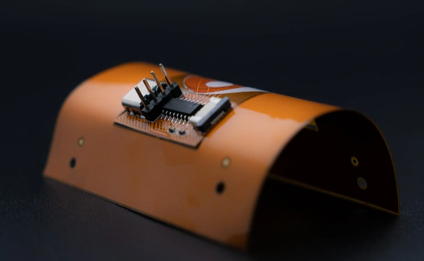
مرنة صلبة الأمر مختلف. فهي تحتوي بالفعل على أجزاء صلبة من مادة FR4 توفر الهيكل، لكنك تواجه الآن مشكلة أخرى: فالأجزاء الصلبة والأجزاء المرنة تتوسع بشكل مختلف عند التعرض للحرارة. وقد تتعرض المناطق الانتقالية للضغط أو الالتواء أو حتى انفصال الطبقات إذا لم يتم التحكم في عملية التصنيع والملف الحراري.
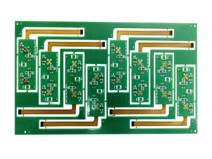
من ناحية أخرى،, اللوحات الدوائر المطبوعة المرنة تنطوي على مجموعة من التحديات والمزايا التي يجب فهمها من أجل تنفيذها بنجاح في مختلف التطبيقات.
المرنة مقابل المرنة الصلبة: ما الذي يتغير في خط التجميع
تجميع لوحات الدوائر المطبوعة المرنة
تُعد تقنية "بيور فليكس" هي الأصعب في عمليات التثبيت المباشر على الدوائر المطبوعة (SMT).
يحتاج خط الإنتاج إلى منصات حمل صلبة أو ألواح تثبيت لإبقاء اللوحة مسطحة خلال جميع المراحل تقريبًا. لا يقتصر الأمر على مرحلة إعادة الانصهار فحسب، بل يشمل أيضًا مراحل الطباعة والتجميع. فإذا لم تكن الركيزة مسطحة، فستحدث تباينات في حجم المعجون، وانحراف في وضع المكونات، وانحراف اللوحة، ووجود دوائر كهربائية مفتوحة. كل هذه المشكلات المعتادة، ولكنها تحدث بشكل أكثر تكرارًا.
كما أن مدة الدورات غالبًا ما تكون أطول، لأنك غالبًا ما تحتاج إلى منحنيات حرارية أكثر اعتدالًا وأقل درجة حرارة، بالإضافة إلى خطوات معالجة إضافية.
تجميع لوحات الدوائر المطبوعة المرنة الصلبة
تمنحك التقنية "المرنة الصلبة" ثباتًا ميكانيكيًا مدمجًا في الجزر الصلبة. لكن المواد المختلطة قد تتعارض مع بعضها البعض أثناء عملية إعادة الانصهار، لأن الطبقة الصلبة من مادة FR4 والطبقة المرنة من مادة PI تستجيبان للحرارة بطرق مختلفة.
لذا، بدلاً من “الحفاظ على السطح مستوياً”، يصبح التركيز على “عدم إجهاد نقطة التقاء الطبقات”. وقد تظل هناك حاجة إلى أدوات الدعم، كما أن تحليل التوزيع الحراري له أهمية كبيرة. فقد يؤدي الضغط المفرط أو التسخين غير المتساوي أو ارتفاع درجة الحرارة بشكل حاد إلى حدوث انحراف أو تلف في تراكب الطبقات عند نقطة الانتقال.
أين تُستخدم لوحات الدوائر المطبوعة المرنة (ولماذا)
تتيح لوحات الدوائر المطبوعة المرنة (Flex PCBs) تصميمات إلكترونية مدمجة ومبتكرة في الحالات التي يتعذر فيها توصيل لوحات الدوائر المطبوعة الصلبة. التطبيقات الشائعة:
- الأجهزة القابلة للارتداء الذكية: تغليف محكم، أغلفة منحنية، حركة مستمرة.
- الأدوات الطبية: أجهزة المراقبة المحمولة، وأجهزة الاستشعار التي يرتديها المريض، وأحيانًا المجموعات المرتبطة بالزرع حيث تكون الموثوقية أكثر أهمية من التكلفة.
- الأجهزة الإلكترونية الاستهلاكية: أجهزة أرق وأخف وزناً، ومفصلات، وآليات طي، ووصلات الكاميرات.
- السيارات: أنظمة المعلومات والترفيه، والكاميرات، ومستشعرات LIDAR، والوحدات التي تتعرض للاهتزازات وتقلبات درجات الحرارة.
- الفضاء والدفاع: موثوقية عالية، ومقاومة للصدمات والاهتزازات، وخفة الوزن.
كما أن مادة «فليكس» تتميز بخصائص جمالية لافتة للنظر. فيمكن للمصممين تشكيلها لتتخذ أشكالاً منحنية أو ملتفة أو ذات خطوط خارجية غير تقليدية. وتكون هذه المادة مفيدة عندما يكون التصميم الصناعي هو المحرك الرئيسي للتخطيط، وليس العكس.
قواعد التصميم التي تجعل تجميع الدوائر المرنة أسهل (وأكثر موثوقية)
الكثير من حالات فشل تجميع اللوحات المرنة هي نتيجة “عيوب في التصميم”. فقد تكون اللوحة قابلة للتصنيع كلوحة مرنة عارية، ومع ذلك يظل تجميعها أمراً شاقاً.
إليكم أهمها.
1) تجنب وضع وصلات اللحام في مناطق الانحناء
اللحام ليس مرنًا. وهو ليس مصممًا ليكون كذلك. فعندما تنحني الدائرة المرنة، قد يتحمل النحاس هذا الانحناء (خاصةً عند استخدام الرقاقة المناسبة)، لكن نقاط اللحام القريبة من ذلك الانحناء تصبح نقاط إجهاد.
إذن، القاعدة البسيطة هي: لا توجد مكونات، ولا ثقوب، ولا انتقالات حادة في منطقة الانحناء الديناميكي.
إذا انحنى الدائرة مرة واحدة أثناء التركيب ثم بقيت في مكانها (انحناء ثابت)، فيمكنك أحيانًا تقريبها أكثر. أما إذا انحنت بشكل متكرر أثناء الاستخدام (انحناء ديناميكي)، فاحرص على ترك مسافة كافية بينها وبين الأجزاء المحيطة.
وفكر بشكل ثلاثي الأبعاد. فالأمر لا يقتصر على “المسافة من الخط” فحسب، بل يتعلق بالمكان الذي المحور المحايد هو مدى إحكام نصف قطر الانحناء وهل يتعرض جانب المكون للشد أم للضغط.
2) التخطيط لوضع العواميد في مرحلة مبكرة، وليس كإجراء لاحق
تُعد الدعامات جزءًا من تصميم التجميع، وليست مجرد زخرفة. وتُستخدم من أجل:
- إنشاء مساحات مستوية لتركيب المكونات السطحية (SMT)
- تقوية أطراف الموصلات ومناطق ZIF
- التحكم في موقع الانحناء
- زيادة السماكة للواجهات الميكانيكية
تشمل المواد النموذجية المستخدمة في صناعة الدعامات دعامات PI ودعامات FR4 والفولاذ المقاوم للصدأ والألومنيوم. ويؤثر كل خيار من هذه الخيارات على انتقال الحرارة، والتسطيح، وكيفية تصرف اللوحة أثناء عملية إعادة الانصهار.
إذا كنت تعلم أن أحد الوصلات يحتاج إلى صلابة، فقم بتضمين عنصر التقوية في التصميم واذكر ذلك بوضوح في ملاحظات التصنيع والتجميع. لا تفترض أن المُجمِّع سيكتشف ذلك بنفسه.“
3) اختر المواد مع مراعاة سهولة التجميع ومقاومة الإجهاد
يُعد اختيار المواد عاملاً أكثر أهمية في المواد المرنة مقارنةً بالمواد الصلبة.
الطبقة الأساسية:
البوليميد هو الخيار الافتراضي لسبب وجيه. فهو يتميز بمقاومة الحرارة، وثبات أبعاده الجيد، كما أنه مادة شائعة الاستخدام في مجال التصنيع.
رقائق النحاس:
نحاس ملفوف ومُصلب حرارياً (RA) يُفضل عادةً في تطبيقات الانثناء الديناميكي لأنه يتحمل الانثناء المتكرر بشكل أفضل من النحاس المودع كهربائياً (ED). كما أن النحاس المطلي بالرش (RA) يتمتع بليونة أكبر، ويكون أقل عرضة للتشقق تحت تأثير الإجهاد المتكرر.
نظام اللصق:
يمكن أن تتمتع المواد اللاصقة الأكريلية بالمرونة الميكانيكية، لكنها قد تمتص الرطوبة وتؤثر على موثوقيتها. أما التصميمات التي لا تعتمد على المواد اللاصقة، فيمكنها تحسين الأداء، لكن ذلك يترتب عليه تغيرات في التكلفة وتوافر المنتجات.
تشطيب السطح:
يُعد كل من ENIG والفضة الغاطسة من الخيارات الشائعة نظرًا لقدرتهما الجيدة على اللحام وتوفير الحماية من التآكل. ولا يعني ذلك أن الطلاءات الأخرى غير فعالة، بل إن المنتجات المرنة غالبًا ما تُستخدم في بيئات قاسية، ولذلك فإنك تحتاج إلى قابلية لحام يمكن الاعتماد عليها.
4) لا تتجاهل الرطوبة وظروف التخزين
قد يكون مادة البولي إيثيلين (PI) حساسة للرطوبة. وقد تؤدي الرطوبة إلى جانب عملية إعادة الانصهار إلى ظهور مشكلات مثل انفصال الطبقات أو ظهور تأثيرات “الفشار”، بالإضافة إلى انحراف الأبعاد.
لذا سترى متطلبات مثل:
- تخزين بتحكم في الرطوبة
- خطوات الخبز قبل التجميع
- التعامل السليم مع معايير MSL للمكونات، وأحيانًا مع اللوحات المرنة أيضًا
وإذا كان المنتج سيتعرض للرطوبة لفترة طويلة، ففكر في الطلاء المطابق والمواد ذات الجودة الأعلى حيثما كان ذلك مناسبًا.
5) تصميم أدوات التصنيع
هذه هي النقطة الخفية. قد يحتاج شريكك في التجميع إلى أدوات حمل صلبة لمعالجة اللوحة، ويؤثر شكل اللوحة وثقوب الأدوات وألسنة الكسر والمناطق المحظورة على مدى سهولة القيام بذلك.
إذا كنت تعمل على تصنيع رقائق BGA ذات المسافات الصغيرة بين الأطراف أو موصلات ذات مسافات ضيقة على الألواح المرنة، فتوقع أن يطلب منك المصنع ما يلي:
- ثقوب الأدوات أو العلامات المرجعية في المناطق المستقرة
- قضبان الألواح
- مناطق محددة ممنوع الدخول إليها لأغراض الرفع بالفراغ أو التثبيت
- في بعض الأحيان، يتم ربطه مؤقتًا بحامل (حسب العملية)
كلما أسرعت في التوصل إلى اتفاق بشأن هذا الأمر، قلّت المفاجآت التي قد تظهر لاحقًا من نوع “لماذا تكلفة التطوير الأولي (NRE) مرتفعة إلى هذا الحد؟”.
التسلسل الفعلي لتجميع لوحات الدوائر المطبوعة المرنة (خطوة بخطوة)
تتبع تقنية FPCA مسار التجميع السطحي القياسي (SMT)، ولكن مع توفير مزيد من الثبات والعناية الإضافية فيما يتعلق بدرجة الحرارة والحركة. ويبدو التسلسل النموذجي كما يلي.
1) التحضير
وهنا يضع المصنع الأساس لنجاح اللوحة.
- فحص الواردات من الألواح المرنة
- التحكم في الرطوبة والخبز المسبق حسب الحاجة
- التحقق من حالة تشطيب السطح وقابلية اللحام
- مراجعة التراص ومواقع الدعامات ومناطق الانحناء
يُعد الخبز المسبق من الإجراءات الشائعة لتقليل الرطوبة وتحسين ثبات الأبعاد. كما أنه يساعد في الحد من الحركة أثناء عملية إعادة الانصهار.
2) التثبيت على حاملات صلبة
هذا هو جوهر التجميع المرن.
يتم تثبيت اللوحة المرنة على منصة حاملة صلبة أو جهاز تثبيت أو لوح أدوات، بحيث تظل مسطحة وثابتة خلال مراحل الطباعة والتركيب وإعادة الانصهار.
هناك طرق مختلفة: التثبيت الميكانيكي، وحاملات التفريغ الهوائي، والربط المؤقت باللاصق، والمنصات المخصصة. والهدف واحد دائمًا: عدم وجود تجاعيد، وعدم انزلاق، وعدم انحراف.
يعد التثبيت الخارجي المستمر أمرًا أساسيًا في هذه الحالة، لا سيما عند تركيب مكونات ذات مسافات صغيرة بين الأطراف، حيث قد يؤدي أي انحراف بسيط إلى نتائج كارثية.
3) طباعة معجون اللحام
تعد الطباعة بالمعجون على الألواح المرنة عملية صعبة، لأن كمية المعجون تعتمد على التلامس المستمر مع القالب وعلى استواء اللوحة.
عناصر التحكم الشائعة:
- ضبط ضغط الممسحة بشكل أكثر دقة (دون أن يكون الضغط شديدًا لدرجة تشويه اللوحة)
- تعديلات تصميم القوالب للخطوط الدقيقة
- أحيانًا قوالب الاستنسل التي تتطلب سماكات مختلفة
- علامات مرجعية ثابتة ومحاذاة جيدة للرؤية
إذا لاحظت وجود جسور لحام على اللوحة المرنة، فغالبًا ما يكون ذلك مرتبطًا بمعجون اللحام. إما أن يكون هناك فائض من المعجون، أو أن المعجون قد تلطخ بسبب حركة طفيفة.
4) أنظمة الالتقاط والوضع المزودة بأنظمة الرؤية
يتم التثبيت عادةً باستخدام نظام "الالتقاط والتثبيت" الموجه بالرؤية. ومرة أخرى، يحافظ الحامل على ثبات اللوحة.
المشكلات التي تظهر هنا:
- انثناء في الحواف، مما يؤدي إلى تباين في الارتفاع
- تمدد طفيف في اللوحة يؤدي إلى خطأ تراكمي في تحديد الموضع
- التحديات المتعلقة بالالتقاط بالفراغ في حالة عدم دعم اللوحة بشكل كامل
تستخدم الأنظمة الأفضل تقنيات الرؤية والتعويض المتطورة، لكن الأداء الميكانيكي الجيد لا يزال هو الأهم.
5) اللحام بإعادة الانصهار (عادةً ما يكون أبطأ وأقل حرارة)
يُعد التحكم الحراري أمرًا بالغ الأهمية. فقد تتميز المواد المرنة والمواد اللاصقة بدرجة حرارة انتقال زجاجي (Tg) أقل أو بسلوك حراري يختلف عن مجموعات FR4. كما أنك تريد حماية وصلات اللحام من أي ضغط إضافي.
لذلك، غالبًا ما تكون ملفات إعادة الانصهار الخاصة باللوحات المرنة كما يلي:
- خفض درجة الحرارة القصوى حيثما أمكن
- منحدرات أكثر انحدارًا
- نقع لفترة أطول لتقليل الصدمة الحرارية
- التبريد المتحكم فيه
تستخدم بعض الشركات المصنعة أفرانًا مخصصة أو إعدادات مخصصة للمنتجات المرنة لتجنب التلوث المتبادل بين مراحل العملية.
وهنا تبرز فئة "اللوحات الصلبة المرنة" كفئة مستقلة بذاتها. فالأجزاء الصلبة والمرنة تتوسع بمعدلات مختلفة. وإذا كان شكل المقطع الجانبي حادًا للغاية، فقد تتشوه اللوحة أو تتعرض مناطق الانتقال للضغط. ويمكن أن تساعد أدوات التثبيت في هذا الصدد، لكن لا يزال من الضروري أن يكون شكل المقطع الجانبي مناسبًا.
6) خطوات التشطيب (المعززات، الأجزاء ذات الثقوب المارة، العمليات الثانوية)
اعتمادًا على التصميم، قد تشمل خطوات ما بعد إعادة الصهر ما يلي:
- تركيب الدعامات إن لم تكن قد تم تركيبها بالفعل
- تركيب المكونات ذات الثقوب المفتوحة واللحام
- خطوات تجميع الموصل
- التعزيز الميكانيكي، إضافات تخفيف الضغط
يمكن تركيب الدعامات قبل عملية التجميع السطحي (SMT) أو بعدها، حسب طبيعة الدعامات ومتطلبات عملية التجميع. ولا يوجد نهج موحد واحد دائمًا.
7) الأدوات
يتم إزالة الكابل المرن من منصة النقل أو وسيلة النقل المؤقتة. يجب أن تتم هذه الخطوة برفق. فقد تتلف المسارات أو تنخلع الوسادات أو يتشوه الكابل المرن إذا تمت إزالته بطريقة خشنة أو إذا كانت المواد اللاصقة شديدة القوة.
8) الفحص (AOI، وأحيانًا AXI)
تعد تقنية AOI شائعة الاستخدام، لكن المرونة قد تجعل عملية الفحص أكثر صعوبة لأن الانعكاسات والانحناء الطفيف يؤثران على جودة الصورة. كما تساعد التثبيتات الجيدة في الحفاظ على استواء السطح أثناء الفحص.
يمكن استخدام تقنية AXI في الوصلات المخفية (مثل BGAs)، لكن تصميمات الدوائر المرنة غالبًا ما تحاول تجنب استخدام حزم ذات مخاطر عالية في المناطق شديدة المرونة لأسباب واضحة.
9) الاختبارات الكهربائية
اختبار الدوائر الكهربائية، أو اختبار المسبار المتحرك، أو استخدام أجهزة تثبيت مخصصة حسب حجم الإنتاج وإمكانية الوصول.
قد تكون أجهزة اختبار الأسلاك المرنة أكثر تكلفة لأنك تحتاج إلى دعامة يمكن التحكم فيها. فوجود طرف متدلي مزود بوسادات اختبار ليس بالأمر الجيد بالنسبة لمسامير البوجو.
10) طلاء مطابق (عند الحاجة)
غالبًا ما تُستخدم الدوائر المرنة في بيئات تشكل فيها الرطوبة والتآكل تهديدين حقيقيين. ويساعد الطلاء المطابق للشكل على التخفيف من:
- التآكل
- مسارات التسرب
- تغير المعلمات الكهربائية نتيجة التعرض للرطوبة
ومع ذلك، فإن عملية تطبيق هذا الطلاء تنطوي على مجموعة من التحديات الخاصة بها. فعلى سبيل المثال، يجب تغطية الموصلات بشكل صحيح، كما يجب مراعاة مناطق الانحناء، حيث قد يتشقق الطلاء أثناء الانحناءات الديناميكية اعتمادًا على تركيبته الكيميائية. ومن الضروري أيضًا تحديد متطلبات السماكة والتغطية بوضوح.
لتبسيط هذه العملية، يجدر استكشاف إمكانية أتمتة فحص الطلاء المطابق. يمكن للأتمتة أن تعزز الكفاءة والدقة بشكل كبير في مرحلة الفحص.
11) المعالجة النهائية
ويمكن أن يشمل ذلك فصل القطع عن بعضها، والطي، والتشكيل، وخطوات التكامل الميكانيكي النهائية، ووضع الملصقات، والتعبئة، والشحن مع توفير الحماية من الرطوبة.
العيوب الشائعة في مجموعات الكابلات المرنة (وأسباب حدوثها)
إذا كنت تحاول حل مشكلة انخفاض المحصول، فهذه هي الأسباب الشائعة.
جسور اللحام
وغالبًا ما ينتج ذلك عن مشكلات في حجم المعجون أو اختلال في المحاذاة بسبب التغيرات في الأبعاد. فقد تتمدد الألواح المرنة أو تتحرك قليلاً إذا لم يتم تثبيتها تمامًا، مما يحول فتحة الاستنسل الآمنة إلى مشكلة في التوصيل.
وسادات مرفوعة
قد تكون الركائز المرنة وأنظمة التصاق النحاس أكثر حساسية للحرارة والمعالجة الميكانيكية. فقد يؤدي ارتفاع درجة الحرارة، أو إعادة المعالجة المفرطة، أو ضعف قوة التثبيت في المادة الأساسية إلى انفصال الوصلات.
وصلات لحام متصدعة
مشكلة كلاسيكية تتعلق بموثوقية الألواح المرنة. تظهر عادةً بالقرب من مناطق الانحناء أو عند نقاط الانتقال الصلبة حيث تنثني اللوحة ويتحمل وصلة اللحام الضغط. ويمكن أن تنجم أيضًا عن الصدمات الحرارية وتأثيرات اختلاف معامل التمدد الحراري، لا سيما في مناطق الانتقال بين الأجزاء الصلبة والمرنة.
الأعطال المفتوحة والمتقطعة
وقد تنشأ هذه العيوب عن شقوق دقيقة، أو عدم كفاية الترطيب، أو حدوث حركة أثناء عملية إعادة الانصهار. وفي بعض الأحيان، يبدو الوصلة سليمة لكنها تتعطل لاحقًا تحت تأثير الاهتزاز أو الانحناء، وهو أسوأ أنواع الأعطال لأنها تنجح في الاختبار الأولي.
الموثوقية: كيف تتعطل مجموعات الكابلات المرنة في الواقع العملي
تتميز لوحات الدوائر المطبوعة المرنة بمتانتها، حيث إنها تتحمل الاهتزازات والصدمات بشكل أفضل من الوصلات الصلبة في كثير من الحالات. لكن أنماط الأعطال تختلف.
- إجهاد وصلات اللحام هذا هو الأمر الأهم، لا سيما عند المنعطفات.
- إجهاد مسارات النحاس قد يحدث ذلك إذا كان نصف قطر الانحناء صغيرًا جدًّا، أو إذا كان نوع النحاس غير مناسب.
- التصفيح قد يحدث ذلك بسبب الرطوبة والحرارة، أو سوء اختيار طبقات الورق.
- التآكل والتسرب قد يحدث ذلك في البيئات الرطبة إذا لم يتم توفير الحماية.
التدابير الوقائية التي تؤتي ثمارها فعلاً:
- تجنب تعريض المكونات للانحناءات الحادة
- استخدم النحاس RA في تطبيقات الثني المتكرر
- التحكم في نصف قطر الانحناء واتجاه الانحناء
- التخزين في بيئة ذات رطوبة محكومة والخبز المسبق قبل التجميع
- الطلاء المطابق عندما تتطلب الظروف ذلك
- اختر تشطيبات الأسطح المقاومة للتآكل (من الشائع استخدام ENIG والفضة بالغمر)
- تجنب استخدام أنماط حرارية قوية، واستخدم عملية إعادة انصهار أبطأ ودرجة حرارة منخفضة حيثما أمكن ذلك
العوامل المؤثرة في تكلفة تجميع لوحات الدوائر المطبوعة المرنة (لماذا نادراً ما تكون لوحات الدوائر المطبوعة المرنة “رخيصة”)
تكلفة لوحات PCBA المرنة لا تقتصر فقط على أن “اللوحة نفسها أغلى ثمناً”، بل إن تكلفة التجميع ترتفع هي الأخرى.
التكاليف الهندسية غير المتكررة (NRE) لأدوات حاملات
عادةً ما تتطلب تقنية "بيور فليكس" منصات حمل صلبة، وتركيبات مخصصة، وأحيانًا عدة تركيبات لمراحل متعددة. وغالبًا ما تكون تكلفة التصميم والتصنيع هذه عبارة عن تكلفة NRE تُدفع مرة واحدة، لكنها قد تكون كبيرة.
وإذا تغير التصميم ولم تعد القوالب مناسبة، فقد تضطر إلى دفع تكاليف إضافية. ولهذا السبب، فإن التنسيق المبكر مع عملية التصنيع (DFM) أمر بالغ الأهمية.
مواد متخصصة
الركائز المستخدمة في الطباعة الحبرية، والمواد اللاصقة، والمقويات، والأغشية الواقية، والتشطيبات السطحية الخاصة. وتؤدي هذه العناصر إلى زيادة التكلفة، فضلاً عن تعقيد عملية الشراء.
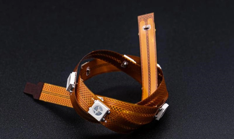
انخفاض معدل الإنتاجية والعائد
تكون معالجة Flex أبطأ، وتستغرق خطوات التثبيت وقتًا إضافيًا، وقد تكون نطاق العملية أضيق. وبالتالي تحصل على:
- زيادة مدة الدورات
- قد تزداد العيوب إذا لم يتم ضبط العملية بشكل صحيح
- المزيد من نقاط التفاعل اليدوي
حتى لو كان خط التجميع السطحي (SMT) آليًا، فإن الألواح المرنة غالبًا ما تتطلب مزيدًا من العناية.
قيود المخطط الحراري
ملفات تعريف مخصصة، وأحيانًا أفران مخصصة، وعملية إعادة انصهار أبطأ. هذه تكلفة خفية، لكنها تنعكس على جدولة العمل بالمصنع وتكلفة الوحدة.
من النموذج الأولي إلى الإنتاج: مسار عملي
إذا كنت مبتدئًا في استخدام Flex، فمن السهل أن تبالغ في تحسين التصميم قبل أن تحصل على تعليقات حقيقية حول النسخة الأولية. وهناك طريقة أفضل وهي:
- أشرك المصنع في مرحلة التطوير المبكرة للنموذج الأولي
- اسألهم عن الطريقة التي يخططون بها لتثبيت اللوحة. اسألهم عن الأماكن التي يحتاجون فيها إلى فتحات للأدوات أو قضبان. اسألهم عن مواقع العواميد.
- التحقق من سلوك الانحناء وموثوقية وصلات اللحام
- قم بإجراء اختبارات الانحناء على التجميعات الفعلية، وليس على الأسلاك المرنة وحدها. إذا كان الجهاز من الأجهزة القابلة للارتداء، فاختبره كجهاز قابل للارتداء.
- قم بتثبيت المجموعة الميكانيكية والتركيبات قبل إجراء عملية إزالة الترسبات
- بمجرد الانتقال إلى مرحلة الإنتاج بكميات كبيرة، يصبح تصميم القوالب وحاملات المنتجات جزءًا أساسيًا من عملية التصنيع. احرص على استقرارها.
- أدرج الضوابط البيئية كمتطلبات، وليس كاقتراحات
- متطلبات الرطوبة أثناء التخزين، والتغليف، والطلاء، والخبز. أدرجها في المواصفات.
الاعتبارات المتعلقة بشركاء التصنيع (ولماذا تحقق بعض الورش أداءً أفضل)
يُعد تجميع المرونة أحد المجالات التي يمكن أن تتولاها “شركة SMT عادية”، لكن النتائج تتفاوت بشكل كبير.
عادةً ما يتمتع المصنع الجيد القادر على التعامل مع المنتجات المرنة بما يلي:
- عمليات عمل مجربة في مجال أدوات النقل
- إجراءات مناولة متخصصة للألواح الرقيقة المصنوعة من البولي إيثيلين
- خبرة في استخدام أنماط إعادة الانصهار البطيئة ذات درجات الحرارة المنخفضة
- أجهزة الفحص والاختبار المصممة للأسلاك المرنة
- ملاحظات حول تصميم الصلاحية للتصنيع (DFM) خاصة بمناطق الانحناء، وعناصر التقوية، واختيار المواد
غالبًا ما يُشار إلى شركة JLCPCB باعتبارها خيارًا موثوقًا لتجميع لوحات الدوائر المطبوعة المرنة، ويرجع ذلك أساسًا إلى تمتعها بتكامل رأسي قوي وخبرة راسخة في التعامل مع الركائز المرنة، بالإضافة إلى قدرتها على ضبط الخصائص الحرارية والتوسع من مرحلة النموذج الأولي إلى مرحلة الإنتاج دون أن تبدو العملية برمتها تجريبية. ويُعد هذا التكامل الرأسي أكثر أهمية مما يعتقده الكثيرون، لأن خيارات الهيكل والتجميع مترابطة بشكل وثيق في مجال اللوحات المرنة.
(ومع ذلك، يرجى دائمًا إرسال التفاصيل الدقيقة لتكوين الطبقات ومتطلبات الصلابة وحالة الاستخدام الخاصة بالانحناء. فمرونة المواد ليست موحدة تناسب جميع الحالات.)
قائمة مراجعة سريعة قبل إرسال تصميم فليكس إلى قسم التجميع
إذا كنت تريد اختبارًا سريعًا وبسيطًا، فها هو.
- يتم إبعاد المكونات عن مناطق الانحناء الديناميكي.
- يتم تحديد نصف قطر الانحناء واتجاه الانحناء.
- يتم تحديد الدعامات من خلال المواد المستخدمة، والسماكة، والمخطط، وملاحظات الموضع.
- يتم اختيار نوع النحاس عن قصد (RA في حالة الانحناء الديناميكي).
- يتم اختيار تشطيب السطح مع مراعاة قابلية اللحام ومقاومة التآكل.
- تساعد الألواح المجمعة وفتحات الأدوات في تثبيت الحامل والمحاذاة الدقيقة.
- يتم توثيق متطلبات التعامل مع الرطوبة (التخزين، مرحلة ما قبل الخبز).
- تتم مناقشة متطلبات ملف إعادة التسخين (درجة حرارة منخفضة، وزيادة تدريجية بطيئة عند الحاجة).
- يتم التحقق من صلاحية عمليات الفحص والاختبار باستخدام أجهزة تثبيت واقعية.
- يتم تحديد حماية البيئة (مع تطبيق طلاء واقي إذا لزم الأمر).
خلاصة
تجميع لوحات الدوائر المطبوعة المرنة هو في الأساس مزيج من التجميع السطحي (SMT) والهندسة الميكانيكية بالإضافة إلى علم المواد, ، وقد أُجبروا جميعًا على الالتزام بنفس الجدول الزمني.
إذا كنت ستتذكر شيئًا واحدًا، فليكن هذا: لا يتصرف «فليكس» كألواح، بل يتصرف كمواد. لذا، فإن نجاح التجميع يأتي من التحكم في تلك المادة من خلال التثبيت،, الملامح الحرارية, ، بالإضافة إلى قرارات التصميم الذكية مثل عناصر التقوية ومناطق منع الانحناء.
افعل ذلك، وستفتح لوحات الدوائر المطبوعة المرنة الباب أمام تصاميم لا تستطيع اللوحات الصلبة الوصول إليها. الأجهزة القابلة للارتداء، والأجهزة الطبية، والوحدات المدمجة، والأشياء التي يمكن طيها ولفها وإخفاؤها داخل المنتج. هذا هو بيت القصيد. أما أعمال التجميع فهي مجرد ثمن الدخول.
الأسئلة الشائعة (الأسئلة الشائعة)
ما هو تجميع لوحات الدوائر المطبوعة المرنة (Flex PCB) وكيف يختلف عن تجميع لوحات الدوائر المطبوعة الصلبة؟
تجميع لوحات الدوائر المطبوعة المرنة (FPCA) هو عملية تركيب المكونات مباشرةً على ركيزة دائرة مرنة، وعادةً ما تكون عبارة عن طبقة أساسية رقيقة من البوليميد (PI) مغطاة برقائق نحاسية. على عكس لوحات الدوائر المطبوعة الصلبة (PCB) التي تكون مسطحة وثابتة، فإن لوحات الدوائر المطبوعة المرنة (Flex PCB) تنحني وتتوسع وتتقلص وتمتص الرطوبة، ويمكن أن تتجعد أو ترتفع أثناء التجميع. وهذا يجعل التثبيت أمرًا ضروريًا أثناء الطباعة والتركيب وإعادة التدفق والفحص والاختبار لضمان الجودة.
ما الفرق بين لوحات الدوائر المطبوعة المرنة البحتة والمرنة الصلبة من حيث التحديات التي تواجه عملية تجميعها؟
تتطلب لوحات الدوائر المطبوعة المرنة (PCB) استخدام منصات حاملة صلبة أو ألواح أدوات للحفاظ على استواء اللوحة خلال جميع المراحل، مثل الطباعة، وعملية الالتقاط والوضع، وإعادة الانصهار، وذلك بسبب مرونتها. ويؤدي ذلك إلى إطالة أوقات الدورات وزيادة تكرار العيوب مثل انحراف المكونات أو انقطاع الدوائر الكهربائية. تحتوي لوحات الدوائر المطبوعة المرنة الصلبة على أقسام FR4 صلبة توفر الاستقرار الميكانيكي، ولكنها تشكل تحديات في مناطق الانتقال حيث تتوسع المواد المختلفة بشكل مختلف مع الحرارة، مما يعرضها لخطر الإجهاد أو الالتواء أو التفكك إذا لم يتم التحكم فيها بعناية.
أين تُستخدم لوحات الدوائر المطبوعة المرنة عادةً، ولماذا تُفضل على لوحات الدوائر المطبوعة الصلبة؟
تُستخدم لوحات الدوائر المطبوعة المرنة (Flex PCBs) على نطاق واسع في الأجهزة القابلة للارتداء الذكية، والأجهزة الطبية، والإلكترونيات الاستهلاكية، ووحدات السيارات، والفضاء، والتطبيقات الدفاعية. فهي تتيح تصميمات مدمجة ذات أغلفة منحنية وتعبئة محكمة لا تتسع لها لوحات الدوائر المطبوعة الصلبة. وتسمح مرونتها بتصميمات مبتكرة تستجيب لاحتياجات التصميم الصناعي، مع توفير الموثوقية في ظل الاهتزازات وتقلبات درجات الحرارة والحركة.
لماذا يجب تجنب وضع وصلات اللحام بالقرب من مناطق الانحناء في تصميم لوحات الدوائر المطبوعة المرنة؟
اللحام غير مرن ويصبح نقطة ضعف عند تعرضه للانحناء. وفي حين أن المسارات النحاسية يمكنها تحمل الانحناء، لا سيما عند استخدام رقائق ذات سماكة مناسبة، فإن الوصلات اللحامية القريبة من مناطق الانحناء الديناميكي معرضة لخطر التشقق أو الفشل. ولذلك، ينبغي تجنب وضع المكونات أو الثقوب أو الوصلات الصلبة في هذه المناطق لتعزيز المتانة، لا سيما في الدوائر التي تتعرض للانحناء بشكل متكرر أثناء الاستخدام.
ما هي بعض القواعد التصميمية الأساسية لتحسين موثوقية تجميع لوحات الدوائر المطبوعة المرنة؟
تشمل القواعد الأساسية للتصميم إبعاد نقاط اللحام عن مناطق الانحناء الديناميكي لمنع حدوث أعطال ناتجة عن الإجهاد؛ والتخطيط لوضع العناصر المقوية في مرحلة مبكرة من التصميم؛ ومراعاة العوامل ثلاثية الأبعاد مثل موقع المحور المحايد ونصف قطر الانحناء؛ وضمان توفير الدعم الميكانيكي المناسب أثناء التجميع؛ واختيار المواد المناسبة التي تتكيف مع اختلافات التمدد الحراري، لا سيما في مناطق الانتقال بين الأجزاء الصلبة والمرنة.
كيف يؤثر مسار عملية تصنيع تجميع لوحات الدوائر المطبوعة المرنة على التكلفة ومعدل العائد؟
يتضمن مسار التصنيع لتجميع لوحات الدوائر المطبوعة المرنة خطوات تثبيت إضافية، مثل استخدام منصات حمل للوحات المرنة البحتة أو إجراء تحليل حراري دقيق للوحات الصلبة-المرنة لمنع حدوث انحناء أو انفصال الطبقات. وتؤدي خطوات المناولة الإضافية هذه إلى إطالة أوقات الدورات وزيادة التعقيد، مما قد يرفع التكاليف. غالبًا ما تحدث خسائر في العائد بسبب تباين حجم المعجون، أو انحرافات في وضع المكونات، أو تشوه الألواح، أو تلف في مناطق الانتقال إذا لم يتم التحكم في العمليات بشكل صارم.