
PCB Design for Testability Review
Build test access into the board before production. FLJ reviews your circuit, PCB layout and intended checks, then recommends changes that make the assembled board easier to connect, exercise and diagnose.

One engineering review, three connected questions
Define the coverage
Test Coverage at Circuit Level
Our PCB DFT review connects test coverage with physical access and circuit control. Early schematic review establishes useful connections and operating states; layout review checks how those connections will be reached on the assembled board.
A power-rail measurement, a digital interconnect check and a sensor-interface test examine different aspects of a board. Each needs a suitable way to apply a stimulus or operating condition and observe the result. The DFT review starts with those intended checks, then examines the design that will support them.
We map the intended checks to the relevant nets, devices and interfaces. This connects the test strategy with the design: which signals can be observed, which can be driven, and which circuit areas still have limited coverage.
Physical probes provide access for selected electrical measurements. On an assembled board, parallel components and connected devices can influence a reading, so reaching both ends of a component does not necessarily make its value independently measurable. Boundary scan can extend digital connection checks where supported devices provide access; functional testing examines powered behavior. Coverage follows the actual circuit and test arrangement.
Illustrative circuit example
For example, a probe on a regulator output can establish the rail voltage at a particular operating point. A load-response check asks a different question. It also needs a way to apply the specified load and measure the output with a suitable reference and measurement setup. An accessible pad supplies one connection; the load, control and measurement arrangement make the intended check possible.
Support useful failure diagnosis
The review also considers failure diagnosis. Access to intermediate power or control nodes can help distinguish a supply problem from a communication problem when a final functional check fails. This gives production engineers more useful information than a single pass/fail indication.
Design for physical access
PCB Test Points and Fixture Access
Test points connect the layout to the equipment that will measure it. FLJ reviews their position, exposed contact area and surrounding clearance against the proposed probing or fixture arrangement.
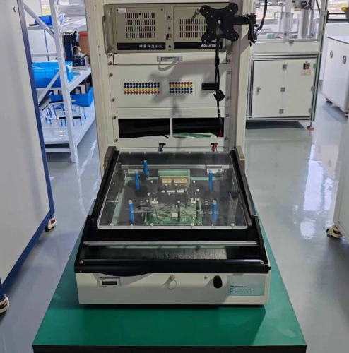
Contact That Remains Accessible
A pad visible in the CAD view may be difficult to reach after assembly. A tall connector can block an approaching probe; a shield or heatsink can cover a point that was accessible earlier in the build. Coating can also cover a contact unless it is masked or the check takes place before coating. Access is assessed for the populated board at the intended test stage.
Pad size, spacing and solder-mask opening work together with probe geometry and positioning tolerance. We assess those relationships for the chosen contact method rather than applying one minimum dimension to every design. Test-point identification and net mapping also help keep the physical contact aligned with the intended measurement.
Support for Repeatable Probing
A bed-of-nails fixture brings many spring contacts onto the board. Locating features establish the board position; mechanical supports help control deflection under the combined contact force. Component placement, probe direction and support locations need to leave room for one another.
The review considers connector access and how the board enters the fixture as well as individual pads. A connection that works on an open bench may become inconvenient when the board is held in a production fixture.
Preserve the Circuit Being Measured
Adding a test point can change the circuit. A long branch on a fast signal creates a stub; added pad and probe capacitance can affect a sensitive node. High-speed, RF and high-impedance circuits need a suitable access approach, not simply more exposed copper.
Power contacts also need attention to the current they carry and their return path. Contact resistance can introduce voltage drop and heating. These electrical effects are considered alongside the mechanical connection.
Make the circuit controllable
Power, Control and Programming Interfaces
Accessible contacts are one part of a testable board. The circuit must also enter a state in which the intended check can be performed.
Power and Operating States
We examine the power, reset, boot and enable arrangements needed to operate the relevant circuit blocks. On a shared signal, an active device may oppose an externally applied test stimulus. A usable test arrangement may need to place that output in a supported high-impedance state or isolate the relevant block. The review identifies how the intended state can be established without relying on an inaccessible signal or an assumption about startup behavior.
Boundary Scan Where Physical Access Is Limited
Boundary-scan cells in supported devices can control and observe digital pins through a JTAG test-access path. This is useful for selected interconnect checks around dense packages where physical probes cannot reach every connection.
The design review considers device support, the scan-chain connection and the states needed for those checks. Available boundary-scan coverage does not automatically establish analog performance or application-level behavior; those questions can need other measurements and functional tests.
An Interface Must Support the Intended Operation
A JTAG connection does not make boundary-scan testing, processor debugging and firmware programming the same task. Each operation depends on the device’s supported access and the tools or routines used with it. SWD access likewise follows the target device and its debug interface.
FLJ reviews the programming connection with the board’s supply and control arrangement so firmware loading can fit the intended build and test sequence. Our IC programming service covers the manufacturing operation; the DFT review addresses whether the design provides usable access for it.
Clear design feedback
DFT Findings and Design Recommendations
We turn the analysis into engineering comments tied to the affected nets, components and layout locations. Each finding connects the test objective with the access or control issue and a recommended correction.
- References to affected nets, components and layout locations
- Explanation of the access or control issue
- Recommended design changes and their purpose
Early schematic review can establish the connections and operating states before routing. A layout review then checks where probes, connectors and fixture supports can reach the assembled board. Revised data can be checked against the findings before the design proceeds to production.
Regulator Enable Connection
- Test objective
- Run the intended powered regulator check.
- Design observation
- The output pad is accessible, but the fixture has no available connection to control the enable signal.
- Recommended action
- Provide a suitable control connection or test mode while retaining the circuit’s required operating behavior.
Illustrative engineering example, not a customer case or a measured test result.
Coverage conclusions describe the selected methods and analysis scope. The review makes remaining gaps visible and supports a practical test plan; it does not turn a list of test points into a guarantee that every possible fault will be found.