


Predgovor
Istraživanje BGA tehnologije započelo je 1960-ih. IBM u Sjedinjenim Američkim Državama prvi ju je koristio. Ali BGA je postala praktična tek početkom 1990-ih.
Tokom 1980-ih, ljudi su željeli manje elektroničke sklopove i više I/O pinova. Tehnologija površinskog montažiranja (SMT) SMT je montaži sklopova omogućio karakteristike kao što su lakoća, tankost, kratkoća i malenost. SMT je također donio veće zahtjeve za razmak pinova i ko-planarnost za komponente sa mnogo izvođača. Međutim, zbog ograničenja u preciznosti obrade, proizvodljivosti, troškova i procesa montaže, ograničenje razmaka za QFP (Quad Flat Pack) komponente je općenito smatranom 0,3 mm. Ovo ograničenje je uveliko sputavalo razvoj montaže visoke gustoće. Također, QFP komponente sa finom razmaknicom zahtijevale su stroge procese sklapanja. To je ograničilo njihovu upotrebu. Iz tog razloga, neke američke kompanije su se fokusirale na razvoj i upotrebu BGA komponenti. Smatrale su da je BGA superioran u odnosu na QFP za potrebe visoke gustoće.
Šta je BGA?
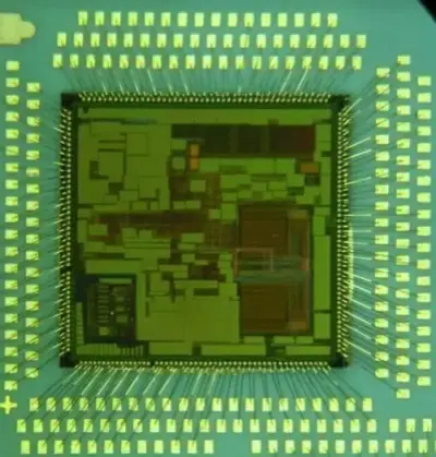
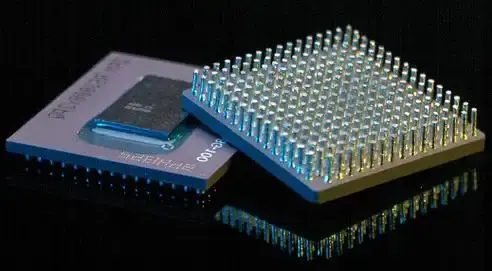
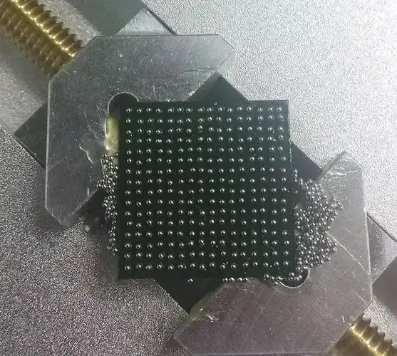
BGA je skraćenica za Ball Grid Array. U ovom pakovanju lemne kuglice su raspoređene u mreži na donjoj strani podloge pakovanja. Ove kuglice služe kao I/O veze između uređaja i štampane pločice (PCB). Komponente pakovane ovom metodom su površinski montirani uređaji. Rani CPU-ovi su koristili DIP pakovanja, kao i neki vrlo osnovni mikrokontroleri danas.
Danas, s brzim rastom elektroničke industrije, računari i mobilni telefoni su uobičajeni. Ljudi žele više funkcija i snažnije performanse od elektroničkih proizvoda, ali također žele manju veličinu i manju težinu. To potiče proizvode prema većem broju funkcija, višim performansama i manjoj veličini. Da bi se postigao ovaj cilj, integrisani krugovi moraju postati manji i složeniji. Zatim raste broj I/O pinova na kolu i raste gustoća I/O pinova u paketu. Da bi se zadovoljio ovaj trend, razvijene su napredne tehnologije pakovanja visoke gustoće. BGA pakovanje je jedna od tih tehnologija.
Među svim vrstama pakovanja integrisanih kola, BGA je zabilježio najbrži rast između 1996. i 2001. godine. Godine 1999. proizvodnja BGA je iznosila oko milijardu jedinica. Do danas je ova tehnologija i dalje uglavnom namijenjena uređajima visoke gustoće i visokih performansi. Nastavlja se razvijati prema finijem pitchu i većem broju ulazno-izlaznih pinova. BGA pakovanje se uglavnom koristi za PC čipsete, mikrorežimere/kontrolere, ASIC-ove, gate array-e, memoriju, DSP-ove, PDA-e, PLD-ove i slične uređaje.
Vrste BGA prema materijalu pakovanja
Ovisno o materijalu pakovanja, BGA uređaji uglavnom uključuju:
PBGA (plastični BGA)
CBGA (keramički BGA)
CCBGA (keramički stupićasti BGA)
TBGA (traka BGA)
CSP (Chip Scale Package ili μBGA)
PBGA — Plastični kuglasti niz za čipove
PBGA koristi BT smolu/stakleni laminat kao podlogu. Pakovanje je zapečaćeno plastikom (epoksidnom livenom smjesom). Lemne kuglice mogu biti olovni legurasi (na primjer 63Sn37Pb, 62Sn36Pb2Ag) ili bezolovni legurasi (na primjer Sn96.5Ag3Cu0.5). Lemne kuglice i tijelo paketa spajaju se bez dodavanja dodatnog kalaja.
Neki PBGA paketi imaju šupljinu. Dolaze u verzijama “šupljina gore” i “šupljina dolje”. Ovi PBGA paketi sa šupljinom poboljšavaju rasipanje toplote i nazivaju se termički poboljšani BGA, odnosno EBGA. Neki ih također nazivaju CPBGA (Cavity Plastic BGA).
Prednosti PBGA:
Dobra toplotna usklađenost s PCB-om. BT smola/stakleni laminat u PBGA ima koeficijent toplotnog širenja (CTE) od oko 14 ppm/°C. Mnogi PCB-ovi imaju CTE oko 17 ppm/°C. Te dvije vrijednosti su bliske. Dakle, toplotna usklađenost je dobra.
Tokom reflow lemljenja, PBGA koristi efekt samopodešavanja kuglica za lemljenje. Površinska napetost rastopljenog kalaja pomaže u poravnavanju kuglica s padovima.
Niska cijena.
Dobri električni performansi.
Nedostatak PBGA:
Osjetljivo na vlagu. Nije pogodno za uređaje koji zahtijevaju hermetičko zaptivanje ili vrlo visoku pouzdanost.
CBGA — keramički BGA paket
CBGA ima najdužu historiju među BGA porodicama. Njegov supstrat je višeslojna keramika. Metalni poklopac je zapečaćen na supstrat pomoću pečatnog kalaja kako bi se zaštitili čip, žičane veze i kontakti. Materijal za kuglice kalaja u pakovanju je visokotemperaturni legur nazvan 10Sn90Pb u izvornom tekstu. Povezivanje između kuglica i tijela pakovanja koristi leguru niže temperature, poput 63Sn37Pb.
Prednosti CBGA:
Dobra hermetičnost i visoka otpornost na vlagu. To osigurava visoku dugoročnu pouzdanost.
Bolja električna izolacija od PBGA.
Veća gustoća pakovanja nego kod PBGA.
Bolja disipacija toplote nego PBGA.
Nedostaci CBGA:
CTE keramičkog podloga i PCB-a znatno se razlikuje. Termička neskladnost je loša. Zamor lemnog spoja je glavni način otkaza.
Viši trošak nego PBGA.
Poravnanje kuglica za lemljenje u blizini ivice paketa postaje teže.
TBGA — Trakašasti niz kuglica na pločici
TBGA je paket sa komorama. Postoje dva načina za povezivanje čipa sa podlogom u TBGA: flip-chip lemljenje i žičano povezivanje. Kod flip-chipa, čip se pričvršćuje na višeslojnu fleksibilnu traku sa vodovima. Periferni niz lemenih kuglica, koje služe kao I/O terminali kola, postavljene su ispod fleksibilne trake. Debeli hermetički poklopac služi i kao hladnjak i kao ojačanje. To čini lemne kuglice ispod fleksibilne podloge ravnoplanarnijim. Čip je pričvršćen za bakreni raspršivač topline unutar komore. Kontakti čipa i kontakti fleksibilne trake povezani su žicama za spajanje. Zaptivni materijal obuhvata čip, žice i kontakte fleksibilne trake (ulijevanjem ili premazivanjem).
Prednosti TBGA:
Fleksibilna traka u pakovanju bolje prati toplinsko širenje štampane pločice.
Reflow lemljenje može koristiti efekt samopodešavanja kalaja. Površinski napon rastopljenih kuglica pomaže u poravnavanju kuglica s padovima.
TBGA je najekonomičniji BGA paket.
Bolja disipacija toplote nego PBGA.
Nedostaci TBGA:
Osjetljiv na vlagu.
Više slojeva materijala u paketu može smanjiti pouzdanost.
Ostale vrste BGA
Ostali oblici paketa uključuju:
MCM-PBGA (Modul sa više čipova PBGA)
μBGA (mikro BGA), paket veličine čipa
SBGA (Stacked Ball Grid Array)
etBGA (extra tanak BGA) gdje je visina paketa oko 0,5 mm, blizu debljine čipa
CTBGA, CVBGA (BGA sa tankim i vrlo tankim nizom čipova) — tanki i vrlo tanki BGAs
Standardna prerada
Načelo standardnih SMD sistema za preradu:
Koriste topli zrak da koncentrišu toplotu na pinove i padove površinskih montažnih uređaja (SMD). To otapa lemne spojeve ili ponovo taloži pastu za lemljenje kako bi se dijelovi mogli ukloniti ili zalemiti. Sistemi za preradu različitih proizvođača razlikuju se uglavnom po izvoru toplote i obrascu strujanja vrućeg zraka. Neke mlaznice ispuhuju vrući zrak iznad SMD-a. Sa stanovišta zaštite uređaja bolje je da zrak cirkuliše oko štampane pločice. Da biste spriječili savijanje štampane pločice, odaberite sistem za preradu koji može predgrijati pločicu.
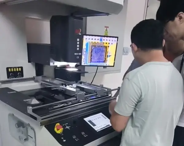
Prerađivanje BGA
Ovaj odjeljak sažima korake prerade BGA koristeći sistem HT996 kao primjer.
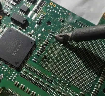
Uklanjanje BGA
Očistite i izravnajte preostali kalaj na padovima štampane pločice pomoću lemilice. Po potrebi koristite kalajnu traku za odlemljivanje i ravnu plosnatu glavu lemilice. Prilikom čišćenja budite pažljivi da ne oštetite padove ili masku za kalaj.
Koristite poseban čistač za uklanjanje ostataka fluksa.
Dehidracija (sušenje)
PBGA dijelovi su osjetljivi na vlagu. Prije sklapanja provjerite je li dio upio vlagu. Ako je vlažan, izvršite pečenje kako biste uklonili vlagu.
Štampanje paste za lemljenje
Pošto su ostale komponente već na ploči, koristite poseban mali BGA šablon. Debljina šablona i veličina otvora zavise od prečnika kuglica i razmaka. Nakon štampe, pregledajte kvalitet otiska. Ako nije dobar, očistite i osušite štampanu ploču, pa ponovo otisnite. Za CSP sa razmakom manjim od 0,4 mm štampanje paste za lemljenje može se preskočiti. U tom slučaju nanesite flukso pastu direktno na kontakte štampane ploče.
Postavite PCB u peć za reflow kako biste uklonili komponentu. Pokrenite program za reflow. Na vrhuncu temperature upotrijebite vakuumsku hvataljku da uklonite komponentu. Ostavite PCB da se ohladi.
Čišćenje podova
Koristite lemilicu i odlemočnu traku za čišćenje i izravnavanje ostataka kalaja na padovima štampane pločice. Pazite da ne oštetite padove ili masku za lemljenje.
Dehidracija (opet)
Pošto je PBGA osjetljiv na vlagu, provjerite i ispecite sve vlažne dijelove prije sklapanja.
Štampanje paste za lemljenje (ponovo)
Kao i prije, koristite mali šablon specifičan za BGA. Debljina šablona i otvor moraju odgovarati veličini kuglica i razmaku. Nakon štampe provjerite kvalitet štampe. Ako nije prihvatljivo, očistite i osušite PCB i ponovo odštampajte. Za CSP s razmakom manjim od 0,4 mm možete preskočiti štampu i nanijeti pastu za flux na kontakte.
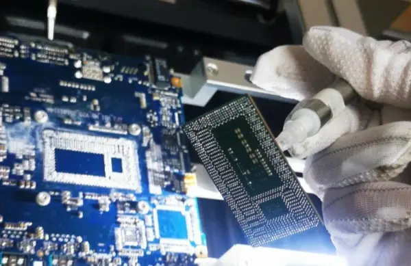
Postavljanje BGA
Ako je BGA nova, provjerite njen sadržaj vlage. Ako je vlažna, ispecite je prije postavljanja.
Općenito, uklonjene BGA komponente mogu se ponovo upotrijebiti. Ali ih prvo treba ponovo obložiti kuglicama. Koraci za postavljanje BGA:
A. Stavite PCB s otisnutom pastom za lemljenje na radni stol.
B. Odaberite odgovarajuću mlaznicu i uključite vakuumsku pumpu. Uzmite BGA mlaznicom, poravnajte dno BGA s padovima PCB-a, spustite mlaznicu i postavite BGA na PCB, zatim isključite vakuum.
Povratno taljenje
Postavite profil reflow-a prema veličini uređaja i debljini PCB-a. Temperature reflow-a za BGA su općenito oko 15 °C više nego za tradicionalne SMD komponente.
Inspekcija
Kvalitet BGA lemnih spojeva obično se provjerava rendgenskom ili ultrazvučnom opremom. Ako nemate tu opremu, koristite funkcionalna testiranja ili iskusne vizualne preglede.
Držite gotovu tiskanu pločicu (PCB) uz izvor svjetlosti i provjerite rubove BGA. Pogledajte prolazi li svjetlost, je li razmak između BGA i PCB-a ravnomjeran sa svih strana, je li pasta za lemljenje potpuno otopljena, je li oblik kuglica za lemljenje ujednačen te koliki je stupanj njihovog srušenja.
Ako spoj nije proziran, može doći do mostovanja ili kuglica kalaja između padova.
Ako je oblik kuglice nepravilan ili iskrivljen, temperatura može biti preniska. Neispravno lemljenje može spriječiti efekt samopodešavanja tokom reflow-a.
Nivo srušavanja kuglica zavisi od temperature reflow-a, količine paste i veličine padova. Uz ispravan dizajn padova, normalno srušavanje nakon reflow-a iznosi otprilike 1/5 do 1/3 visine kuglica prije reflow-a. Ako je srušavanje preveliko, temperatura je previsoka i može doći do mostovanja.
Ako razmak između ivica BGA i PCB-a nije jednak, temperatura oko paketa nije bila ravnomjerna.
Proces reballinga (pribavljanje kalajnih kuglica)
Uklonite preostali kalaj sa donjih padova BGA i očistite.
Upotrijebite lemilicu da uklonite preostali kalaj s padova na tiskanoj pločici. Koristite dekalajnu traku i ravnu vrh lemilice. Pazite da ne oštetite padove ili masku za kalaj.
Koristite poseban čistač za uklanjanje ostataka fluksa.
Štampajte flukso na donjim padovima BGA.
Često se koristi viskozni fluks zbog svojstava prianjanja i pomoći pri lemljenju. Osigurajte da su otisnuti uzorci fluksa jasni i da se ne šire. Ponekad se umjesto fluksa koristi pasta za lemljenje. Ako se pasta koristi, sastav metala u pasti mora odgovarati metalu kuglica za lemljenje.
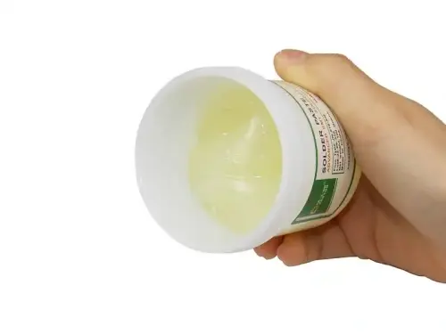
Za štampanje koristite mali specijalni BGA šablon. Debljina i otvor šablona moraju odgovarati prečniku kuglica i razmaku. Nakon štampanja provjerite kvalitet štampe. Ako nije dobar, očistite i ponovo odštampajte.
Odaberite kuglice za lemljenje
Prilikom odabira lemnih kuglica uzmite u obzir materijal i promjer kuglica. Za PBGA lemne kuglice obično se koriste 63Sn/37Pb, isti legur koji se koristi u reflow lemljenju. Zato odaberite kuglice istog legura kao i kuglice uređaja.
Izbor veličine kuglica je važan. Ako koristite fluks visoke viskoznosti, odaberite kuglice istog prečnika kao kuglice uređaja. Ako koristite pastu za lemljenje, odaberite kuglice nešto manje od kuglica uređaja.
Priključak za loptu
Postoji nekoliko metoda za pričvršćivanje loptica:
A) Metoda mašine za loptice
Ako imate mašinu za kuglice, odaberite šablonu koja odgovara rasporedu BGA padova. Otvor šablone treba biti 0,05–0,1 mm veći od prečnika kuglice. Ravnomjerno pospite kuglice po šabloni. Protresite mašinu za kuglice tako da višak kuglica sklizne u posudu za sakupljanje, ostavljajući tačno jednu kuglicu u svakoj rupi.
Postavite šablonu na radni stol. Uzmite vakuumskom mlaznicom otisnutu BGA s flukom ili premazanu pastom. Poravnajte i spustite BGA na kuglice u šabloni tako da pasta ili fluk drže kuglice na padovima uređaja. Koristite pincetu da držite okvir uređaja i isključite vakuum. Postavite uređaj kuglicama okrenutim prema gore na stol. Provjerite nedostajuće kuglice i dodajte ih pincetom po potrebi.
B) Šablonska metoda
Postavite BGA obloženu flukom ili pastom na radni stol, tako da strana s flukom gleda prema gore. Pripremite šablonu koja odgovara rasporedu BGA padova. Otvor šablone treba biti 0,05–0,1 mm veći od prečnika kuglice. Poduprite šablonu duž rubova pomoću podloški tako da udaljenost od BGA bude jednaka ili nešto manja od prečnika kuglice. Poravnajte pod mikroskopom. Ravnomjerno pospite kuglice po šabloni. Uklonite višak kuglica pincetom tako da u svakoj rupi ostane po jedna kuglica. Uklonite šablonu i provjerite, nadopunjujući sve nedostajuće kuglice.
C) Ručno postavljanje
Postavite BGA obložen flukom ili pastom na radni stol. Koristite pincetu ili olovku za podizanje, kao kod uobičajenog postavljanja SMD-a, da biste postavili kuglice jednu po jednu.
D) Metoda štampanja paste za lemljenje
Uradite šablonu debljom i blago povećajte otvor. Štampajte pastu za lemljenje direktno na BGA kontakte. Površinska napetost će formirati kuglice kalaja nakon reflow-a.
Ponovni protok
Pokrenite reflow da pričvrstite kuglice kalaja na uređaj.
Čišćenje i rukovanje nakon lemljenja
Nakon reballinga temeljito očistite BGA uređaj. Zatim ga sastavite i zalemite što je prije moguće. Time se sprječava oksidacija kuglica kalaja i upijanje vlage u uređaj.
Sažetak
Uz kontinuirane napretke u tehnologiji, moderan život je usko povezan s elektronikom. Sitni mobilni telefoni, mali radio uređaji, prijenosna računala, memorije, tvrdi diskovi, CD uređaji i televizori visoke rezolucije zahtijevaju miniaturizaciju i malu težinu. Da bismo to postigli, moramo raditi na proizvodnim procesima i komponentama.
SMT (Surface Mount Technology) je pratio ovaj trend i postavio temelje za lagane, tanke, kratke i male elektroničke proizvode. Otkako je SMT sazrio 1990-ih, trendovi u elektroničkim proizvodima prema prenosivosti, miniaturizaciji, umrežavanju i multimediji dodatno su potaknuli tehnologiju montaže. Pojavile su se nove metode montaže visoke gustoće. BGA je jedna od metoda montaže visoke gustoće koja je dosegla praktičnu primjenu. Ovaj članak je predstavio karakteristike BGA montaže i kontrolu kvaliteta lemnih spojeva.