


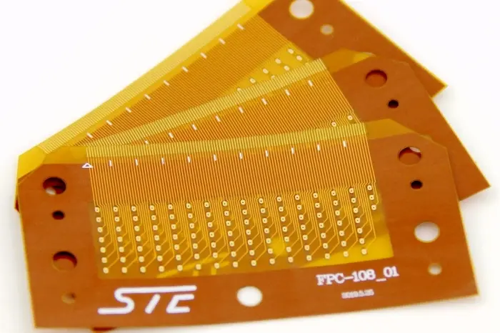
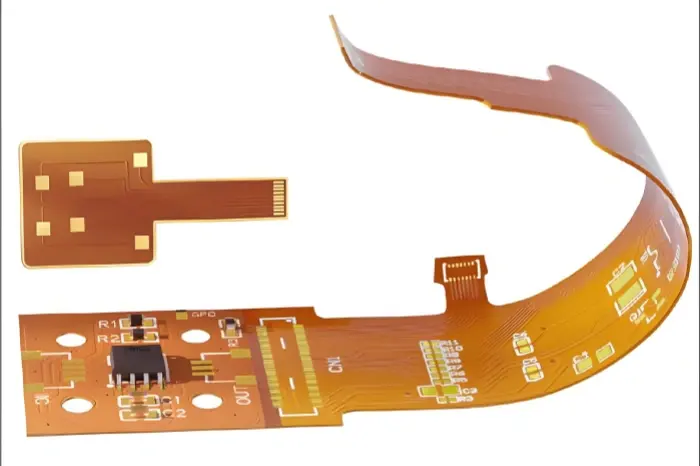
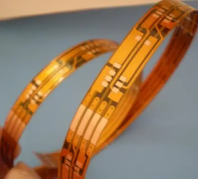
Bảng mạch in dẻo còn được gọi là bảng mạch in linh hoạt, mạch dẻo hoặc bảng mạch dây dẻo. Như tên gọi đã chỉ ra, đây là loại bảng mạch có thể uốn cong. Nó có thể gập lại, cuộn tròn, kéo giãn và di chuyển theo ba chiều. Bảng mạch in dẻo được chế tạo trên một lớp màng mỏng như polyimide hoặc polyester. Chúng mang lại độ tin cậy cao và tính linh hoạt rất tốt.
Mạch in dẻo (FPC) có nguồn gốc từ những năm 1950, khi các nhà nghiên cứu tại Hoa Kỳ phát triển các kỹ thuật in và khắc các dây dẫn phẳng lên các chất nền dẻo như một giải pháp thay thế cho các cụm dây dẫn truyền thống. Các nhà sản xuất đã sử dụng màng polyester hoặc polyimide làm nền. Những loại màng này giúp bảng mạch trở nên chắc chắn và có thể uốn cong. Bằng cách tích hợp mạch điện lên các tấm nhựa mỏng, nhiều linh kiện nhỏ có thể được xếp chồng lên nhau trong không gian hẹp. Kết quả là một mạch điện có thể uốn cong, gấp lại và phù hợp với các hình dạng nhỏ gọn. Mạch điện linh hoạt có trọng lượng nhẹ, chiếm ít không gian, tản nhiệt tốt và dễ lắp đặt. Chúng đã khắc phục những hạn chế của các phương pháp kết nối cũ.
Mạch linh hoạt bao gồm ba nhóm vật liệu chính. Thứ nhất là lớp màng cách điện. Thứ hai là chất dẫn điện. Thứ ba là chất kết dính. Các thành phần này phối hợp với nhau để đáp ứng nhu cầu về các thiết bị điện tử nhỏ gọn và di động. Mạch linh hoạt giúp các thiết bị trở nên nhỏ gọn hơn, tinh vi hơn và đáng tin cậy hơn.
Các vật liệu được sử dụng trong bảng mạch in dẻo
1. Màng cách nhiệt
Lớp màng cách điện tạo thành lớp nền chính cho mạch. Chất kết dính được sử dụng để dán lá đồng lên lớp màng cách điện. Trong các thiết kế mạch dẻo nhiều lớp, lớp màng này cũng được sử dụng để dán các lớp bên trong lại với nhau.
Lớp màng cách điện bảo vệ mạch khỏi bụi và độ ẩm. Nó cũng giúp giảm lực căng khi bảng mạch bị uốn cong. Lớp dẫn điện được làm từ lá đồng.
Một số mạch in dẻo sử dụng các bộ phận cứng làm từ nhôm hoặc thép không gỉ. Các bộ phận cứng này giúp đảm bảo độ ổn định kích thước. Chúng cung cấp sự hỗ trợ vật lý cho các linh kiện và dây dẫn. Ngoài ra, chúng còn giúp giảm ứng suất. Các bộ phận cứng được dán vào mạch in dẻo bằng keo dán.
Một loại vật liệu phổ biến khác là lớp liên kết phủ lên cả hai mặt của màng cách điện. Lớp liên kết này có tác dụng cách điện và giúp kết dính các lớp lại với nhau. Nó có thể giúp loại bỏ nhu cầu sử dụng một số lớp màng và cho phép các nhà sản xuất kết dính nhiều lớp với ít linh kiện hơn.
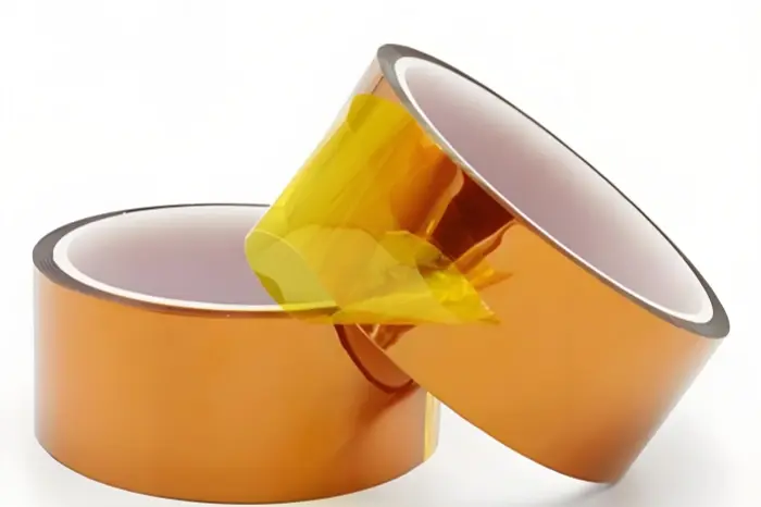
Có nhiều loại màng cách điện. Các loại được sử dụng phổ biến nhất là màng polyimide và màng polyester. Khoảng 80% các nhà sản xuất mạch in dẻo tại Mỹ sử dụng màng polyimide. Khoảng 20% sử dụng màng polyester.
Polyimid không dễ cháy. Chất liệu này giữ nguyên hình dạng, chống rách và chịu được nhiệt độ hàn. Polyester, còn được gọi là PET (polyethylene terephthalate), có các đặc tính vật lý gần giống với polyimide. Chất liệu này có hằng số điện môi thấp hơn và hấp thụ ít độ ẩm hơn. Tuy nhiên, nó không chịu được nhiệt độ cao tốt bằng. Polyester nóng chảy ở khoảng 250°C và có nhiệt độ chuyển pha thủy tinh (Tg) khoảng 80°C. Điều này hạn chế việc sử dụng nó trong các sản phẩm cần hàn mép bảng mạch nặng. Trong các ứng dụng ở nhiệt độ thấp, polyester có thể trở nên cứng. Tuy nhiên, polyester vẫn phù hợp cho điện thoại và các sản phẩm khác không phải đối mặt với điều kiện khắc nghiệt.
Màng polyimide thường được kết hợp với keo polyimide hoặc keo acrylic. Màng polyester thường được kết hợp với keo polyester.
2. Người dẫn chương trình
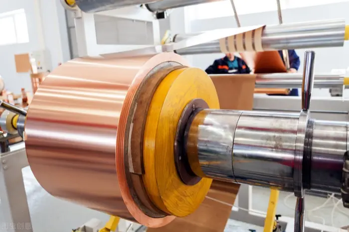
Tấm đồng là vật liệu phù hợp cho mạch in dẻo. Tấm đồng có thể được sản xuất bằng phương pháp mạ điện (ED) hoặc cán và ủ (RA). Một mặt của tấm đồng mạ điện có bề mặt bóng. Mặt còn lại có bề mặt mờ. Tấm đồng mạ điện có thể uốn cong và có nhiều độ dày và chiều rộng khác nhau. Mặt mờ của tấm đồng mạ điện thường được xử lý đặc biệt để tăng khả năng bám dính.
Đồng RA vừa dẻo dai vừa mịn màng. Loại đồng này có thể có độ bền cao hơn. Đồng RA rất hữu ích trong các thiết kế yêu cầu uốn cong nhiều lần hoặc cần độ dẻo dai động.
3. Chất kết dính
Chất kết dính không chỉ có tác dụng gắn màng cách điện vào dây dẫn. Chúng còn có thể đóng vai trò là lớp phủ, lớp bảo vệ hoặc lớp phủ bề mặt. Điểm khác biệt chính nằm ở cách thức thi công lớp này. Lớp phủ bám dính vào màng cách điện và tạo thành cấu trúc nhiều lớp.
In lụa được sử dụng để phủ keo và tráng lớp. Không phải tất cả các cấu trúc ghép lớp đều sử dụng keo. Các tấm ghép không dùng keo tạo ra các mạch mỏng hơn và linh hoạt hơn. Chúng cũng có khả năng truyền nhiệt tốt hơn so với các tấm ghép sử dụng keo. Do không có lớp keo cản trở nhiệt, nhiệt được truyền qua mạch hiệu quả hơn. Điều này cho phép các mạch linh hoạt không dùng keo hoạt động trong những điều kiện mà các mạch linh hoạt sử dụng keo có thể bị hỏng.
Các bước hàn cho FPC (Quy trình hàn FPC)
Dưới đây là các bước thực hành để hàn tay chip PQFP và các linh kiện SMD thông dụng trên mạch in dẻo. Hãy sử dụng các bước này làm hướng dẫn chi tiết. Đồng thời, hãy tuân thủ các quy tắc an toàn và phòng ngừa tĩnh điện (ESD).
Trước khi hàn, hãy bôi chất trợ hàn lên các điểm tiếp xúc. Dùng mỏ hàn để xử lý các điểm tiếp xúc. Điều này giúp tránh tình trạng mạ thiếc không đều hoặc các điểm tiếp xúc bị oxy hóa. Các chip thường không cần xử lý trước.
Dùng nhíp để đặt cẩn thận chip PQFP lên bảng mạch in (PCB). Thực hiện thao tác này để tránh làm cong hoặc gãy các chân chip. Căn chỉnh chip sao cho khớp với các điểm tiếp xúc. Đảm bảo chip được đặt đúng hướng. Làm nóng mỏ hàn lên trên 300°C. Cho một ít hàn lên đầu mỏ hàn. Dùng dụng cụ ấn mạnh vào chip đã được căn chỉnh. Cho một lượng nhỏ hàn vào hai chân đối diện nhau. Giữ chip và hàn hai chân đối diện nhau. Thao tác này sẽ cố định chip tại vị trí. Sau khi hai chân này được hàn, kiểm tra lại vị trí. Nếu cần, di chuyển hoặc tháo chip ra và đặt lại.
Khi bắt đầu hàn tất cả các chân, hãy bôi chì hàn lên đầu mỏ hàn. Bôi chất trợ hàn lên tất cả các chân để giữ cho chúng luôn ẩm. Chạm đầu mỏ hàn vào đầu mỗi chân cho đến khi thấy chì hàn chảy vào chân. Giữ đầu mỏ hàn song song với các chân trong quá trình hàn. Điều này giúp ngăn chặn hiện tượng các chân bị nối chập do lượng chì hàn quá nhiều.
Sau khi hàn xong tất cả các chân, hãy dùng chất trợ hàn để làm ướt các chân và làm sạch lớp hàn. Loại bỏ phần hàn thừa để tránh ngắn mạch và cầu hàn. Cuối cùng, dùng nhíp để kiểm tra các mối hàn bị lỗi. Khi hoàn tất, hãy làm sạch bảng mạch. Dùng cồn và bàn chải cứng, sau đó chà theo hướng các chân cho đến khi hết cặn hàn.
Điện trở và tụ điện SMD dễ lắp đặt hơn. Đặt linh kiện lên miếng đệm. Sau đó, đặt một đầu lên miếng đệm và giữ chặt bằng kẹp nhíp. Hàn một đầu trước. Kiểm tra vị trí. Nếu đã thẳng hàng, hãy hàn đầu còn lại.
Những điểm khác biệt chính giữa bảng mạch in cứng và bảng mạch in dẻo
Bảng mạch in cứng (PCB cứng) chính là loại bảng mạch mà mọi người thường nghĩ đến. Chúng sử dụng các chất dẫn điện và các linh kiện khác trên một tấm nền không dẫn điện. Tấm nền không dẫn điện này thường chứa thủy tinh. Thủy tinh giúp tấm nền trở nên chắc chắn và cứng cáp. Bảng mạch in cứng cung cấp độ ổn định tốt cho các linh kiện và có khả năng chịu nhiệt cao.
Bảng mạch in dẻo (PCB) cũng có các đường dẫn điện trên một lớp nền không dẫn điện. Tuy nhiên, lớp nền này có tính dẻo, chẳng hạn như polyimide. Lớp nền dẻo cho phép mạch uốn cong, chịu được rung động, tản nhiệt tốt và gấp lại thành nhiều hình dạng khác nhau. Nhờ những đặc tính này, mạch in dẻo hiện nay được sử dụng phổ biến trong các thiết kế điện tử nhỏ gọn và tiên tiến.
Ngoài vật liệu cơ bản và độ cứng, những điểm khác biệt lớn khác bao gồm:
Lựa chọn vật liệu dẫn điện: Flex thường sử dụng đồng RA mềm hơn thay vì đồng ED cứng. Điều này rất hữu ích trong trường hợp mạch điện cần uốn cong mà không bị nứt.
Sản xuất: Các nhà sản xuất PCB dẻo không sử dụng lớp chống hàn như PCB cứng. Họ sử dụng lớp phủ bề mặt (coverlay) hoặc lớp phủ bảo vệ (covercoat) để bảo vệ các đường mạch trần.
Chi phí: Mạch dẻo thường có giá cao hơn mạch cứng. Tuy nhiên, mạch dẻo giúp các kỹ sư thu nhỏ kích thước sản phẩm. Điều này có thể làm giảm tổng chi phí sản phẩm vì sản phẩm có kích thước nhỏ hơn thường có chi phí sản xuất hoặc vận chuyển thấp hơn.
Cách lựa chọn giữa bảng mạch in cứng và bảng mạch in dẻo
Cả hai loại đều có thể được ứng dụng trong nhiều sản phẩm. Tuy nhiên, một số ứng dụng lại phù hợp hơn với một loại cụ thể. Ví dụ, bảng mạch in cứng (PCB) thường được sử dụng trong các sản phẩm cỡ lớn như tivi và máy tính để bàn. Trong khi đó, các sản phẩm nhỏ gọn như điện thoại di động và thiết bị đeo thường cần đến mạch in dẻo.
Khi đưa ra quyết định, hãy cân nhắc:
Sản phẩm của bạn cần phải làm được gì.
Mức giá mà ngành thường áp dụng cho các sản phẩm tương tự.
Việc sử dụng một loại vật liệu có thể ảnh hưởng như thế nào đến chi phí hoặc quy trình lắp ráp.
Nếu thiết bị của bạn cần có khả năng gập, uốn cong hoặc tiết kiệm không gian, hãy chọn loại dẻo. Nếu bạn cần chi phí thấp và độ bám dính cao cho các bộ phận có kích thước lớn, hãy chọn loại cứng.
Các thanh gia cố cho bảng mạch in dẻo
Các tấm gia cố còn được gọi là tấm gia cường, tấm đỡ hoặc thanh gia cường. Chúng được sử dụng trong lĩnh vực điện tử để kiểm soát độ uốn cong. Các tấm gia cố giúp khắc phục nhược điểm là bảng mạch uốn cong có thể quá mềm. Chúng làm cho các khu vực cắm linh kiện trở nên chắc chắn hơn và hỗ trợ quá trình lắp ráp.

Các loại thanh gia cố phổ biến:
Các thanh gia cố bằng thép không gỉ
Các thanh gia cố bằng nhôm
Miếng gia cố bằng polyester
Các tấm gia cố bằng polyimide
Các thanh gia cố bằng sợi thủy tinh
Các thanh gia cố bằng PTFE (Teflon)
Các thanh gia cố bằng polycarbonate
Quy tắc xử lý các thanh gia cố bằng polyimide (PI):
Nên nung các thanh gia cố PI ở nhiệt độ 80°C trong 30 phút trước khi sử dụng.
Nếu có thể, hãy làm việc trong phòng sạch ở nhiệt độ khoảng 25°C và độ ẩm tương đối 65%.
Hãy sử dụng các thanh gia cố PI mới cắt ngay. Nếu để quá một ngày, hãy bọc kín chúng lại.
Làm sạch bề mặt tiếp xúc giữa FPC và tấm gia cố trước khi dán.
Hãy đảm bảo các điều kiện dán và ép phù hợp khi sử dụng các loại máy ép khác nhau.
Sau khi đông cứng, hãy đợi khuôn nguội hẳn trước khi mở ra và lấy chi tiết ra.
Không làm nguội các thanh gia cố PI quá nhanh sau khi ép lớp. Nếu cần thiết, hãy chuyển chi tiết sang một vật liệu dẫn nhiệt chậm như vải sợi thủy tinh. Nếu sử dụng máy ép tấm, hãy đợi cho đến khi sản phẩm nguội xuống nhiệt độ phòng.
Cách phòng ngừa vết lõm và vết nứt trên bảng mạch in dẻo
Trục uốn trung tính của mạch uốn có thể không nằm chính giữa trong chồng mạch. Việc xử lý đúng cách sẽ giúp tránh bị lõm và nứt.
Bảng mạch in dẻo vừa là bộ phận cơ khí vừa là bộ phận điện. Cách bố trí đường mạch phải đảm bảo độ bền cho toàn bộ mạch. Khác với bảng mạch cứng, bảng mạch dẻo có thể uốn cong, xoắn và gập lại để vừa vặn bên trong sản phẩm hoàn thiện. Nếu độ uốn cong vượt quá giới hạn nhất định, lớp đồng sẽ phải chịu lực căng lớn. Điều này có thể làm gãy bảng mạch dẻo hoặc gây ra các vết lõm.
Vật liệu linh hoạt mang lại cho các nhà thiết kế những lựa chọn mà bảng mạch cứng không có. Ngay cả khi vật liệu linh hoạt là lựa chọn phù hợp cho công việc, điều đó không có nghĩa là các đường dẫn đồng sẽ không bao giờ bị hỏng. Đồng cũng có giới hạn về mức độ căng thẳng mà nó có thể chịu đựng.
Bạn cần lưu ý nhiều yếu tố, đặc biệt là khi sản phẩm phải chịu lực uốn động (uốn cong trong quá trình sử dụng) hoặc khi nó phải gấp gọn vào các không gian lắp đặt hẹp. Độ chính xác là yếu tố quan trọng để tránh nứt vỡ.
Các yếu tố cần xem xét trong thiết kế nhằm nâng cao
uốn cong và uốn dẻo
Dưới đây là những ý tưởng thiết kế rõ ràng nhằm nâng cao tuổi thọ và độ tin cậy.
Nắm rõ các điểm chịu lực và bán kính uốn
Hãy nắm rõ các giới hạn về uốn cong, gấp và xoắn. Đối với dây cáp uốn một mặt, nếu độ giãn hoặc lực ép vượt quá bán kính uốn hoặc điểm chịu lực, đồng sẽ bị nứt. Luôn đảm bảo làm việc trong phạm vi các giới hạn này.
Trục trung tính
Đối với các ứng dụng uốn cong động, thiết kế mạch in một mặt là lựa chọn tối ưu. Thiết kế một mặt giúp lớp đồng có không gian để nằm gần tâm cấu trúc. Với bố trí này, lớp đồng sẽ không bị nén hoặc kéo căng quá mức trong quá trình uốn cong động.
Càng mỏng càng tốt
Các lớp mỏng hơn dễ uốn cong hơn. Chúng có bán kính uốn cong bên trong nhỏ hơn và lực căng tác động lên lớp ngoài ít hơn. Đối với các bộ phận phải uốn cong nhiều, hãy sử dụng đồng mỏng hơn và các lớp điện môi mỏng hơn.
Bố trí dầm chữ I
Cấu trúc I-beam có nghĩa là các lớp đồng hoặc lớp điện môi chồng lên nhau trực tiếp ở cả hai mặt. Điều này giúp tăng cường độ bền cho vùng gấp. Do lớp bên trong bị nén lại, lớp bên ngoài sẽ phải chịu lực kéo lớn hơn. Để giảm thiểu hiện tượng này, hãy bố trí các đường dẫn điện lệch nhau ở hai mặt đối diện.
Các góc uốn cong hoặc nếp gấp gấp khúc
Nhiều bảng mạch dẻo được thiết kế để có thể gập lại. Một bảng mạch được chế tạo tốt có thể chịu được lần gập hoặc xoắn đầu tiên. Tuy nhiên, việc liên tục gập lại vùng đã bị nhăn là không tốt. Lớp đồng sẽ bị đứt theo thời gian. Điều này không được khuyến khích. Hãy sử dụng các thủ thuật thiết kế như đường mạch có góc bo tròn ở vùng gập.
Một số mẹo khác để tránh nứt:
Sử dụng các đường mạch hàn hoặc mạ thiếc.
Sử dụng đồng RA hoặc đồng ED có hướng hạt được kiểm soát.
Sử dụng màng polyimide phủ ở khu vực uốn cong.
Sử dụng các thanh gia cố ở mặt dưới và một lớp phủ ở mặt trên.
Các lưu ý thực tiễn khác về thiết kế và quy trình
Khi lắp các bộ phận, hãy đảm bảo các đường mạch không đi qua các lỗ và các cạnh sắc nhọn. Điều này giúp giảm nguy cơ hỏng hóc.
Sử dụng các hình dạng miếng đệm tròn và thêm các góc bo tròn vào các đường dẫn gần các điểm uốn cong.
Tránh đặt các lỗ vias trong các vùng uốn cong chịu lực lớn. Nếu bắt buộc phải đặt các lỗ vias, hãy sử dụng vật liệu gia cố.
Hãy sử dụng các góc bo tròn cho đường mạch và điểm tiếp xúc. Các góc vuông sẽ làm tập trung ứng suất và có thể gây ra vết nứt.
Khi bố trí đường mạch qua một nếp gấp, hãy cố gắng bố trí chúng vuông góc với trục gấp nếu có thể. Điều này giúp giảm ứng suất kéo.
Đối với các chuyển động lặp lại, hãy thử sử dụng hiệu ứng chuyển tiếp từ uốn cong sang bảng mạch sao cho phần uốn cong nằm trong khu vực trống, không có linh kiện hay lỗ dẫn điện.
Hướng dẫn lắp ráp và lưu ý về môi trường
Bảo quản polyimide và các vật liệu khác trong túi kín, khô ráo. Độ ẩm có thể làm hỏng chất kết dính và gây bong tróc.
Giữ cho khu vực làm việc luôn sạch sẽ. Bụi và dầu mỡ có thể làm giảm độ bám dính.
Đối với hàn nóng chảy, hãy tuân thủ các giới hạn về thời gian và nhiệt độ của vật liệu. Polyimide chịu được nhiệt độ cao, nhưng polyester thì không.
Khi sử dụng chất kết dính, hãy tuân thủ các đường cong đóng rắn và các bước làm mát. Làm mát quá nhanh có thể gây ra ứng suất và biến dạng.
Hãy sử dụng thiết bị chống tĩnh điện khi thao tác với các mạch in dẻo. Một số mạch có chứa các vi mạch nhạy cảm.
Các ứng dụng phổ biến của bảng mạch in dẻo
Mạch in dẻo được sử dụng rộng rãi trong nhiều sản phẩm:
Điện thoại di động và máy tính bảng
Máy ảnh
Thiết bị đeo
Thiết bị y tế và cảm biến
Cảm biến ô tô và các bộ phận bảng điều khiển
Điện tử hàng không vũ trụ và quân sự
Đèn LED và màn hình LED
Đầu nối và cụm cáp
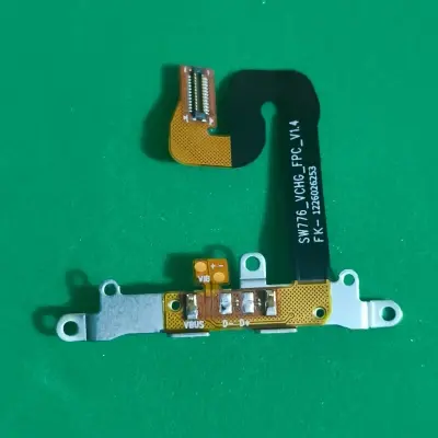
Những ưu điểm chính của chúng là kích thước nhỏ gọn, trọng lượng nhẹ và khả năng thích ứng với các hình dạng bất thường.
Ưu điểm và hạn chế của mạch linh hoạt
Ưu điểm:
Tiết kiệm không gian và giảm trọng lượng.
Cho phép có các bộ phận có thể di chuyển hoặc gập lại.
Giảm nhu cầu về đầu nối do có thể nối dây cáp mềm giữa các bo mạch.
Hiệu suất tản nhiệt tốt nếu được thiết kế đúng cách.
Độ tin cậy được nâng cao trong nhiều ứng dụng động.
Giới hạn:
Chi phí cao hơn so với các bảng mạch in cứng thông thường.
Việc xử lý đòi hỏi sự cẩn thận hơn.
Một số vật liệu không chịu được nhiệt độ hàn cao.
Nếu thiết kế không đúng, có nguy cơ xảy ra hiện tượng uốn động trong thời gian ngắn.
Kiểm tra và đánh giá chất lượng
Để đảm bảo độ tin cậy:
Sử dụng thử nghiệm uốn để kiểm tra tuổi thọ uốn động.
Sử dụng phương pháp thay đổi nhiệt độ theo chu kỳ để kiểm tra khả năng chịu đựng sự thay đổi nhiệt độ.
Kiểm tra bằng tia X hoặc kính hiển vi để phát hiện các vết nứt ẩn.
Thực hiện các thử nghiệm kéo trên các thanh gia cố và bộ nối được dán keo để kiểm tra độ bền kết dính.
Kiểm tra trở kháng và tính liên tục của các đường truyền tín hiệu.
Những lưu ý cuối cùng và mẹo nhanh
Hãy chọn polyimide nếu cần khả năng chịu nhiệt cao hơn và độ tin cậy cao hơn. Hãy chọn polyester nếu chi phí thấp hơn và khả năng chịu nhiệt thấp hơn là chấp nhận được.
Để đạt được độ uốn dẻo linh hoạt, hãy sử dụng các lớp mỏng một mặt và đồng RA.
Thêm các thanh gia cố tại các vị trí nối để hỗ trợ quá trình lắp ráp.
Hãy giữ bán kính uốn cong càng lớn càng tốt. Bán kính lớn hơn giúp tăng tuổi thọ.
Nếu phát hiện sớm các vết lõm hoặc vết nứt, hãy kiểm tra vị trí uốn cong và phần chồng lớp. Hãy thay đổi loại đồng, độ dày hoặc thêm một lớp phủ bảo vệ.
Hãy đảm bảo các bước lắp ráp phù hợp với giới hạn của vật liệu. Ví dụ: không sử dụng quy trình hàn nhiệt độ cao trên mạch linh hoạt làm từ polyester.