Ghi chú này giải thích lý do tại sao các bảng mạch in (PCB) có thể thay đổi kích thước trong quá trình gia công và cách kiểm soát điều này. Từ quá trình chuyển mẫu lớp trong đầu tiên trên bảng mạch in (PCB) Vật liệu nền PCB, Qua nhiều chu kỳ ép laminate và sau đó là quá trình chuyển mẫu lớp ngoài, bảng mạch có thể giãn nở hoặc co lại khác nhau theo các hướng X và Y. Bằng cách xem xét sơ đồ quy trình sản xuất PCB hoàn chỉnh, chúng ta có thể xác định các bước quy trình và nguyên nhân dẫn đến hiện tượng giãn nở bất thường của bảng mạch hoặc sự không đồng nhất về kích thước.
1. Nguyên nhân chính gây ra sự giãn nở và co ngót kích thước của PCB
1.1 Ổn định nguyên liệu đầu vào và tính nhất quán giữa các lô
Yếu tố chính là độ ổn định kích thước của vật liệu nền PCB đầu vào. Cần đặc biệt chú ý đến độ nhất quán của vật liệu giữa các chu kỳ ép laminate từ cùng một nhà cung cấp. Ngay cả khi mỗi lô vật liệu đáp ứng tiêu chuẩn kỹ thuật, sự không nhất quán giữa các lô có thể gây ra vấn đề. Ví dụ, một bảng thử nghiệm đầu tiên có thể được điều chỉnh với bù đắp lớp trong hợp lý. Sau đó, khi sản xuất sử dụng một lô vật liệu nền khác, kích thước mẫu cuối cùng có thể vượt quá giới hạn dung sai.
Có một trường hợp bất thường khác. Một số lô sản phẩm cho kết quả X-quang và tỷ lệ chuyển lớp ngoài bình thường sau khi lamination lớp ngoài. Tuy nhiên, sau đó, trước khi thực hiện quá trình định tuyến viền, tấm panel được phát hiện đã bị co lại. Trong một trường hợp sản xuất, một số lô sản phẩm cho thấy hiện tượng co lại nghiêm trọng sau quá trình chuyển lớp ngoài. Độ rộng của tấm panel so với chiều dài đơn vị vận chuyển, tương ứng với tỷ lệ chuyển lớp ngoài, đã co lại tới 3,6 mil trên mỗi 10 inch. Chúng tôi đã truy vết lô hàng này. Dữ liệu X-quang sau khi lamination lớp ngoài và tỷ lệ chuyển lớp ngoài vẫn nằm trong giới hạn kiểm soát. Hiện tại, hệ thống kiểm soát quy trình không có phương pháp giám sát đáng tin cậy để phát hiện sớm loại biến động này.
1.2 Các yếu tố thiết kế của hệ thống panel (mảng)
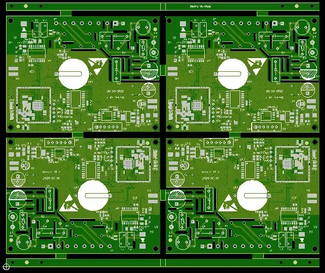
Các bảng mạch tiêu chuẩn thường được thiết kế với bố cục đối xứng. Khi tỷ lệ chuyển đổi bình thường, bố cục đối xứng không ảnh hưởng nhiều đến kích thước mẫu cuối cùng. Tuy nhiên, một số khách hàng hoặc nhà thiết kế sử dụng bố cục bảng mạch không đối xứng để cải thiện hiệu quả sử dụng vật liệu và giảm chi phí. Bố cục không đối xứng có thể gây ra sự khác biệt rõ rệt về kích thước mẫu giữa các khu vực khác nhau trên bảng mạch. Trong quá trình gia công, bạn có thể gặp vấn đề về kiểm soát đăng ký cho các bảng mạch không đối xứng. Điều này áp dụng cho các bước như khoan lỗ mù bằng laser, phơi sáng lớp ngoài, phơi sáng lớp phủ hàn và in ký hiệu. Trong các bước này, các bảng mạch không đối xứng khó căn chỉnh và cải thiện hơn so với các bảng mạch đối xứng.
1.3 Hệ số truyền tải mẫu lớp trong đầu tiên
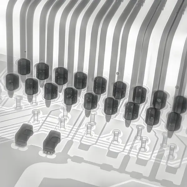
Bước chuyển giao mẫu lớp trong đầu tiên là bước quan trọng quyết định kích thước cuối cùng của PCB. Nếu việc điều chỉnh tỷ lệ phim hoặc bù đắp phim cho quá trình chuyển giao lớp trong đầu tiên không chính xác, kích thước mẫu PCB hoàn thiện có thể không đáp ứng yêu cầu của khách hàng. Việc điều chỉnh tỷ lệ lớp đầu tiên sai cũng có thể gây ra các vấn đề sau này. Ví dụ, các lỗ vi mạch mù (blind vias) có thể không khớp với các pad tiếp đất của chúng. Điều này có thể làm giảm độ cách điện giữa các lớp và thậm chí gây ra chập điện. Nó cũng có thể gây ra các vấn đề về định vị cho các lỗ vi mạch xuyên qua (through vias) hoặc lỗ vi mạch mù (blind vias) trong quá trình chuyển giao lớp ngoài.
2. Phương pháp giám sát và cải thiện có mục tiêu
Dựa trên phân tích trên, chúng ta có thể áp dụng các phương pháp giám sát và cải thiện cụ thể.
2.1 Giám sát tính ổn định kích thước của nguyên liệu đầu vào và tính nhất quán của lô sản phẩm.
- Kiểm tra định kỳ. Thường xuyên kiểm tra độ ổn định kích thước của vật liệu cơ bản từ các nhà cung cấp khác nhau. Theo dõi sự khác biệt về chiều dọc và chiều ngang (X và Y) giữa các lô vật liệu cùng loại. Sử dụng thống kê cơ bản để phân tích dữ liệu kiểm tra. Điều này giúp xác định các nhà cung cấp có vật liệu ổn định hơn theo thời gian.
- Sử dụng dữ liệu để lựa chọn nhà cung cấp. Cung cấp dữ liệu kích thước cho SQE (Kỹ thuật Chất lượng Nhà cung cấp) và bộ phận mua hàng. Điều này cung cấp bằng chứng tốt hơn cho việc lựa chọn nhà cung cấp.
- Phát hiện các biến động nghiêm trọng. Đối với các lô hàng kém chất lượng gây ra sự suy giảm nghiêm trọng sau khi chuyển lớp ngoài, phương pháp phát hiện duy nhất hiện nay là đo lường các tấm sản phẩm đầu tiên tại giai đoạn định tuyến hoặc kiểm tra tại giai đoạn xem xét xuất hàng. Phương pháp sau yêu cầu kiểm soát lô hàng nghiêm ngặt. Trong sản xuất hàng loạt với nhiều lô hàng, việc nhầm lẫn có thể xảy ra và điều này làm cho việc phát hiện trở nên khó khăn hơn.
2.2 Sử dụng thiết kế bảng đối xứng khi có thể
- Quy tắc thiết kế. Nên áp dụng thiết kế bảng mạch đối xứng. Đối xứng giúp duy trì sự giãn nở và co ngót đồng đều trên tất cả các đơn vị được giao trong bảng mạch.
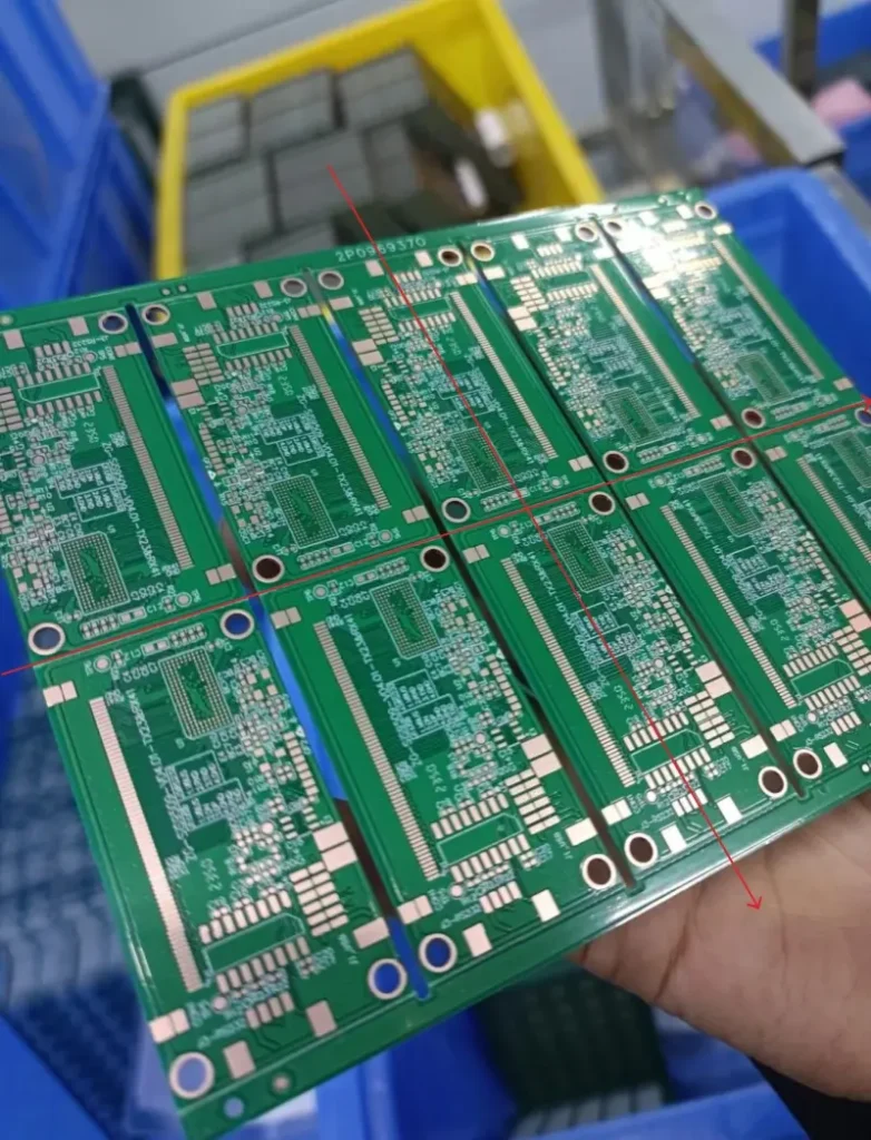
- Ghi chú vị trí các đơn vị trên bảng mạch. Nếu có thể, yêu cầu khách hàng cho phép sử dụng các dấu hiệu biên quá trình như vết ăn mòn hoặc văn bản in để đánh dấu vị trí của từng đơn vị được vận chuyển trên bảng mạch. Đối với các thiết kế không đối xứng, việc đánh dấu này sẽ hữu ích hơn. Nếu sau này một đơn vị trên bảng mạch có kích thước bất thường hoặc lỗi pad đáy của lỗ mù cục bộ, bạn có thể xác định đơn vị lỗi và loại bỏ nó trước khi vận chuyển. Điều này giúp tránh các sự cố lắp ráp và khiếu nại từ phía khách hàng.
2.3 Tạo bảng thử nghiệm để thiết lập tỷ lệ chuyển đổi và xác minh.
- Tạo một bảng thử nghiệm quy mô. Làm một bảng thử nghiệm ban đầu để xác định tỷ lệ thu nhỏ phim chính xác cho quá trình chuyển lớp trong đầu tiên. Bước này rất quan trọng khi bạn thay đổi vật liệu nền hoặc nhà cung cấp phim P để giảm chi phí hoặc vì các lý do khác.
- Xử lý các bảng mạch không đạt tiêu chuẩn một cách cẩn thận. Nếu phát hiện các bảng mạch không đạt tiêu chuẩn, hãy kiểm tra xem các lỗ via của đơn vị có phải từ quá trình khoan thứ cấp hay không. Đối với các bảng mạch tuân theo quy trình khoan thông thường, bạn có thể chuyển chúng sang quá trình chuyển lớp ngoài và điều chỉnh tỷ lệ phim theo nhu cầu. Tuy nhiên, đối với các bảng mạch có lỗ khoan thứ cấp, hãy xử lý các bảng mạch bất thường với sự cẩn thận đặc biệt. Bạn phải đảm bảo kích thước mẫu hoàn thiện và khoảng cách từ mục tiêu đến lỗ via (đục lỗ thứ cấp) đáp ứng tiêu chuẩn. Giữ lại hồ sơ: thu thập dữ liệu tỷ lệ của bảng đầu tiên cho các bảng lamination thứ cấp để có cơ sở tham khảo.
2.4 Điều khiển quá trình bằng dữ liệu đăng ký lớp trong bằng tia X
- Sử dụng đăng ký tia X. Sau khi ép laminate, sử dụng đo đạc tia X của các mục tiêu lớp trong trên bảng mạch để thu thập dữ liệu đăng ký cho vị trí các lỗ khoan. So sánh các số liệu đo đạc của các mục tiêu lớp trong này với dữ liệu bảng mẫu đã được chấp nhận. So sánh này cho thấy liệu kích thước bảng mạch có bị giãn nở hoặc co lại bất thường hay không.
- Độ dung sai thu nhỏ chặt chẽ. Phân tích lý thuyết cho thấy độ thu nhỏ ở đây cần được kiểm soát trong khoảng ±0.025% để đáp ứng yêu cầu kích thước cho các tấm panel tiêu chuẩn. Giữ độ dung sai chặt chẽ để tránh các vấn đề về đăng ký sau này.
3. Tóm tắt và Lời khuyên cuối cùng
Bằng cách phân tích các nguyên nhân chính gây ra sự giãn nở và co lại của kích thước PCB, chúng ta có thể xác định các điểm theo dõi thực tế và phương pháp cải tiến. Các hành động chính là:
• Kiểm tra và theo dõi tính ổn định của nguyên liệu đầu vào giữa các lô sản xuất.
• Ưu tiên bố cục bảng điều khiển đối xứng và thêm dấu vị trí khi bố cục phải không đối xứng.
• Sử dụng bảng thử nghiệm để thiết lập tỷ lệ thu nhỏ lớp phim trong cùng đầu tiên và ghi lại dữ liệu.
• Sử dụng đăng ký tia X sau khi ép laminate để phát hiện sớm sự thay đổi kích thước.
• Xử lý các tấm panel có lỗ khoan thứ cấp một cách khác biệt và với sự kiểm tra kỹ lưỡng hơn.
Tôi hy vọng các chuyên gia trong lĩnh vực PCB sẽ thấy những ý tưởng này hữu ích. Hãy kết hợp các phương pháp này với điều kiện sản xuất của riêng bạn. Sau đó, hãy chọn những cải tiến phù hợp với nhà máy và sản phẩm của bạn. Nếu bạn muốn, tôi có thể chuẩn bị một danh sách kiểm tra ngắn gọn hoặc một mẫu biểu cho việc kiểm tra vật liệu và ghi chép về bảng mạch thử nghiệm mà bạn có thể sử dụng trực tiếp tại xưởng sản xuất.
4. Ưu điểm của Philifast trong việc kiểm soát kích thước PCB và ổn định quy trình
4.1 Năng lực sản xuất và kiểm soát chất lượng
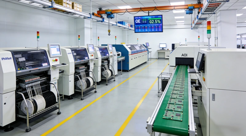
Philifast có những ưu điểm thực tiễn nổi bật trong việc kiểm soát sự thay đổi kích thước PCB và cung cấp các bo mạch ổn định, đáng tin cậy. Công ty đã hoạt động trong nhiều năm và sử dụng các dây chuyền sản xuất tiên tiến cùng các công cụ kiểm tra hiện đại. Philifast sở hữu các chứng chỉ chất lượng quan trọng và vận hành một đội ngũ kỹ sư lành nghề chuyên xử lý bo mạch thử nghiệm, kiểm tra nguyên vật liệu đầu vào và thiết lập quy trình sản xuất. Philifast có nhiều SMT Dây chuyền, kiểm tra tia X, kiểm tra AOI và SPI, và một quy trình kiểm tra đầy đủ. Bo mạch in (PCBA) dòng, tất cả đều giúp phát hiện và ngăn chặn các vấn đề về kích thước và đăng ký ngay từ giai đoạn đầu của quy trình.
4.2 Các biện pháp kiểm soát quy trình và tích hợp dịch vụ
Philifast áp dụng các kiểm tra nghiêm ngặt đối với vật liệu đầu vào, ghi lại dữ liệu đo lường bảng mẫu và sử dụng đăng ký tia X để theo dõi các mục tiêu lớp trong sau khi lamination. Các bước này giúp giảm thiểu rủi ro co ngót hoặc giãn nở sau này và dễ dàng phát hiện các đơn vị lỗi trong bảng mạch trước khi xuất xưởng. Philifast cũng cung cấp dịch vụ PCB và PCBA trọn gói từ giai đoạn mẫu đến sản xuất hàng loạt, do đó cùng một đội ngũ thiết lập mẫu bảng mạch có thể theo dõi quá trình lắp ráp và kiểm tra để đảm bảo kết quả nhất quán.