PCB Component Layout Principles
In PCB layout design, the placement of components is critical. It affects how neat the board looks and the length and number of printed traces. It also affects the overall reliability of the device. The following are several basic rules that PCB component placement should follow.
Even and Consistent Distribution
Place components so they are spread evenly over the whole board. Keep density and spacing consistent. Do not let components completely fill the board. Leave some space around the board edges. How big the empty margin should be depends on the board area and how the board is fixed in the product. Components that sit right on the PCB edge should be at least 3 mm from the board edge. In electronic instruments, it is common to leave 5 to 10 mm of space along each edge.
In general, place components on one side of the PCB when you can. Each wire lead of a component should use its own solder pad.
No Overlap and Adequate Clearance
Components should not overlap from top to bottom in a way that causes crossing. Keep a sufficient gap between adjacent components. The gap must not be too small to avoid physical contact. If two nearby components have a large potential difference, maintain a safe distance between them. In ordinary environments, a safe air gap is about 200 V per mm. That is, if you expect high voltage differences, increase spacing.
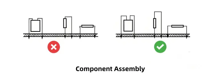
Low Mounting Height
Make the mounting height of components as low as possible. The lead of a component should not stand more than about 5 mm above the board. If parts sit too tall, they resist vibration and shock poorly. Tall parts can tilt, fall over, or touch neighboring components. This lowers reliability.
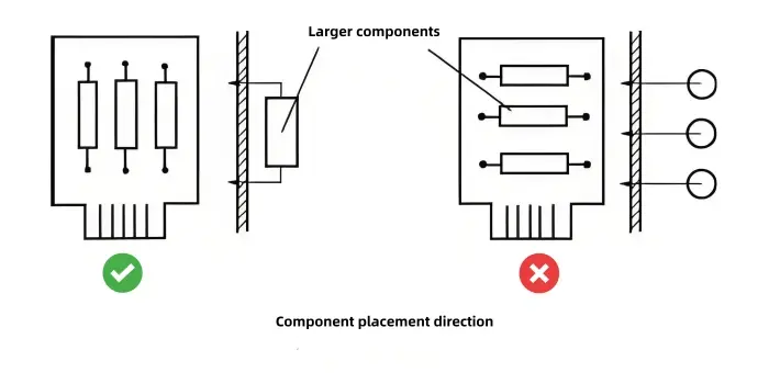
Axis Direction and Regularity
Decide component axis directions according to how the PCB will sit and be fixed in the final product. For regular arrays of components, align the axis of large parts so they stand upright relative to the product. This improves mechanical stability on the board. Aligning axes helps keep parts fixed under vibration.
Pad Spacing and Lead Bends
Pads on both ends of a component should be slightly wider apart than the axial body length of the component. When bending leads, do not bend right at the root. Leave some straight lead length before bending—at least 2 mm—to avoid damaging the body. This reduces stress on the component lead and the solder joint.
How Components Are Mounted and Fixed on PCB
There are two main mounting styles for components on a PCB: vertical (upright) and horizontal (lying down). Horizontal means the component axis is parallel to the PCB surface. Vertical means the axis is perpendicular. Both methods have pros and cons. Use them flexibly when you design. You can use one style or a mix of both. Make sure the circuit resists vibration, is easy to service, and the component layout is even. That will also help when routing traces.

Vertical (Upright) Mounting
Vertically mounted components take less board area. You can fit more parts per unit area. This is good for dense product designs like portable radios and hearing aids. Many small portable instruments use vertical mounting.
However, vertical parts should be small and light. Large or heavy parts are not suitable for vertical mounting. Heavy parts reduce mechanical strength and lower vibration resistance. They may tilt or fall and touch other parts, causing reliability problems.
Horizontal (Lying Down) Mounting
Horizontal mounting gives better mechanical stability. It makes the board look neater. Horizontal mounting increases the component span between solder pads, which makes it easier to route a trace between the two solder points. That is helpful for trace layout. Horizontal mounting is generally preferred when mechanical stability and ease of routing are important.
PCB Component Arrangement Formats
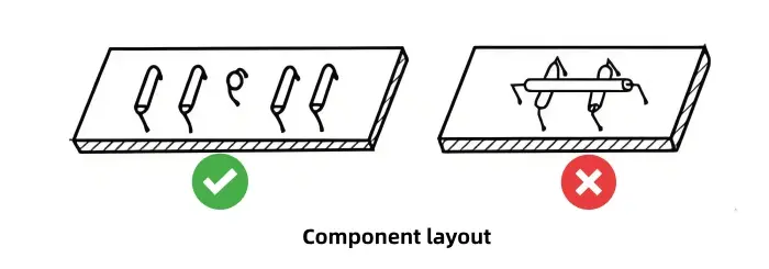
Components should be placed evenly, neatly, and compactly on the board. Try to reduce and shorten interconnections between circuit units and between individual components. There are two main layout formats on a PCB: irregular placement and regular placement. You can use either one alone or both together.
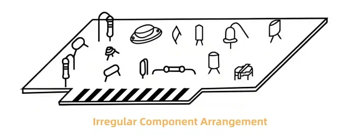
Irregular Placement
In irregular placement, component axes are not aligned and their positions follow no strict rule. This looks disordered, but it frees component orientation and position. That freedom often makes trace layout easier. It can shorten or reduce interconnections, greatly lowering total trace length. Shorter traces lower parasitic parameters and help reduce interference. Irregular placement is very useful for high frequency circuits. It is often used with vertically mounted components.
Regular Placement
Regular placement aligns the axes of components so they are parallel or perpendicular to the board edges. Except for high frequency parts, most electronic products should try to place components either parallel or perpendicular. This is especially true when components are mounted horizontally. Regular placement improves board appearance and makes assembly, soldering, and debugging easier. It is also easier for production and maintenance.
Regular placement is ideal for low frequency circuits with moderate component types but large quantities. Many instruments use this format. But regular placement places constraints on position and direction. Trace routing may become more complex, and total trace length may increase as a result.
Positioning of Component Pads on PCB
Each lead of a component must occupy a solder pad on the PCB. Pad position depends on the component size and how it is fixed. For vertical mounting or irregular placement, pad position can be less constrained by component size and spacing. For regular placement, pad positions and spacing should follow certain standards.
In any method, pad centers (that is, the center of the plated hole) should not be too close to the board edge. The typical distance is 2.5 mm or more. At least the pad center should be greater than the board thickness away from the edge.
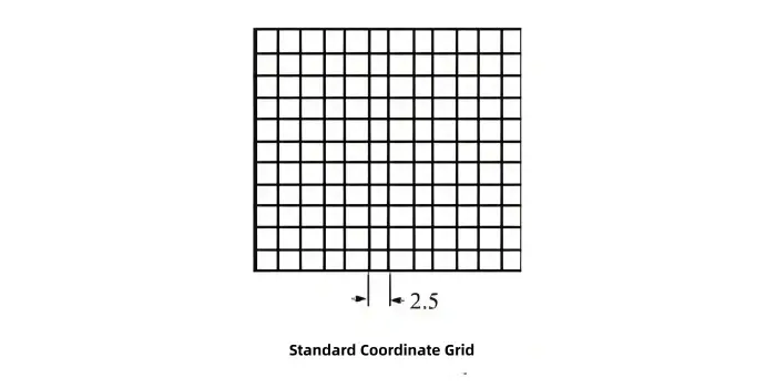
Pad positions should ideally fall on a standard coordinate grid.
In the IEC standard, the basic grid pitch is 2.54 mm (domestic standard is 2.5 mm). Sub-grid pitches include 1.27 mm or 0.635 mil (1.25 mm or 0.625 mil). These grid standards matter when using computer aided design, automatic drilling, or automatic component placement and soldering. For manual drilling, aside from dual in-line IC pin spacing, you may relax strict grid adherence. Still, pad positions should keep components neat and consistent. For parts with similar sizes, try to keep pad spacing uniform. Pad center distance should not be less than the board thickness. This keeps things neat and makes assembly and lead bending easier.
Of course, neatness is relative. For special cases use judgment.

Factors That Affect PCB Layout
Many factors influence a good PCB layout. Here we cover the most important ones.
Signal Flow Direction
When arranging circuit units on a board, divide the whole circuit by function. Place functional modules in order of the signal flow. This makes layout convenient for signal paths. Try to keep signal directions consistent. In most cases arrange signal flow from left to right (input on the left, output on the right) or top to bottom (input at top, output at bottom).
Place components that connect directly to input and output connectors near those connectors. Layout around the core device of each functional block. For example, use a transistor or an IC as the core, then place related components around it. Consider part shape, size, polarity, and number of pins. Adjust position and orientation to shorten wiring.
Location of Special Components
Interference in electronic equipment can come from many sources: electrical, magnetic, thermal, and mechanical. When designing the board layout, first analyze the circuit schematic. Identify special components first, then place other parts. That way you avoid interference and take steps to reduce it as much as possible.
Special components are those that impact the device electrically, magnetically, thermally, or mechanically. They may also be parts that must be fixed at certain places due to operation requirements.
Electromagnetic Interference (EMI) Prevention
EMI happens often in working equipment. Causes include external electromagnetic waves and poor routing or bad component placement on the PCB. Many interference problems can be avoided in the layout phase. If you ignore this early, the design may fail.
Separate or shield parts that can affect each other. Shorten connections in high frequency sections to reduce distributed parameters and mutual electromagnetic coupling. If you plan to use metal shielding cans for RF sections, leave board area for the shield size.
Sensitive parts should not be too close to noisy parts. Separate high-voltage (e.g., 220 V) and low-voltage sections, and separate input and output stages. If DC power leads are long, add filtering parts to stop 50 Hz noise.
If some components or traces may have high potential differences, enlarge spacing to avoid discharge or breakdown. Avoid metal-cased parts touching each other. For example, the metal case of an NPN transistor or the heatsink of a power transistor may be connected to the collector, which could be at high potential. Electrolytic capacitor cans often are at negative potential or ground. If these metal cases are not insulated, ensure enough distance or add insulation, otherwise a short can occur.
Thermal Interference Control
Temperature rise also causes interference. In layout, identify which parts generate heat and which are temperature sensitive.
Place heat-generating parts, like high-power resistors, near the enclosure or where airflow is good. Use vents to help cooling. Do not cluster heat parts together. Consider heatsinks or a small fan to keep temperature rise within limits. Large power parts can be anchored to the chassis to use the metal shell for heat dissipation. If they must be on the PCB, give them large heatsinks and keep them away from other parts.
Temperature-sensitive parts such as transistors, ICs, and large electrolytic capacitors should not be near heat sources or at the top of the device where temperature rises more. Prolonged heating changes operating points and can degrade performance.
Mechanical Strength Considerations
Mind the board’s balance and stability. For big and heavy parts (power transformers, large electrolytic capacitors, power transistors with heatsinks), do not only rely on PCB solder joints. Mount them to the chassis when possible so the center of gravity is low and the product is stable. Large components can warp the PCB or damage other components and connectors.
If a component weighs more than about 15 g and must be on the PCB, do not rely only on solder. Use brackets, clamps, or other mechanical supports.
For boards larger than about 200 mm × 150 mm, the board will face bending and vibration stress. Add a mechanical frame or stiffener to prevent deformation. Leave space for mounting brackets, locating screws, and connector attachments.
Serviceability and Accessibility
For adjustable parts like potentiometers, variable capacitors, or tuning coils, consider how the product will be adjusted. If adjustment is from outside, match the part position to the knob on the front panel. If adjustment is internal, place the component for easy access on the PCB.
For safety in debugging and service, place high-voltage parts where hands are less likely to touch. For instance, place CRT high-voltage components where they are hard to reach.
Summary of PCB Layout
Layout is the main part of PCB design. Correctly arranging parts on a fixed board area is the first step. Layout is not only connecting components by printed lines per the schematic. To make a reliable product, place parts and their connections thoughtfully.
If layout is poor you can get interference or poor performance and the theoretical design may fail. Some layouts meet technical specs but look messy. Uneven, disorderly placement not only reduces visual quality, it makes assembly and maintenance harder. That is not a reasonable design.
The guidelines above aim to teach basic PCB layout knowledge for ordinary printed circuits. Follow them to make layout as reasonable as possible. Good layout reduces trace length, lowers interference, improves mechanical durability, helps cooling, and eases manufacturing and maintenance.
Practical Checklist for PCB Layout (Quick Reference)
- Divide the circuit into functional blocks and place blocks following the signal flow.
- Place input and output related parts near the connectors.
- Place high-frequency blocks compactly and keep their traces very short.
- Separate high-voltage and low-voltage areas.
- Reserve room for metal shields if needed.
- Keep heat-generating parts near ventilation or chassis.
- Keep temperature-sensitive parts away from heat sources.
- Use vertical mounting for dense, small parts. Use horizontal mounting for stability and easier routing.
- Maintain at least 3 mm from component pads to board edge when parts are at the board edge; typical pad center to edge clearance ≥ 2.5 mm.
- Use standard grid spacing when you plan automated assembly (2.54 mm or 2.5 mm).
- Keep pad center spacing not less than board thickness.
- For heavy parts, use mechanical supports in addition to solder.
- Add stiffeners or frames for large boards (> 200 × 150 mm).
- Leave space for testing points and service access.
- Ensure component axes align for neatness when possible, but choose irregular layout for RF to reduce trace length.