
Immersion Tin PCB Manufacturing
A thin, flat tin surface for fine-pitch soldering and specified press-fit connections.
FLJ supplies immersion-tin PCBs from bare-board fabrication through component assembly. Vertical and horizontal finishing routes accommodate different board sizes and thicknesses, with selective finishes for separate soldering and contact areas.
How We Manufacture Immersion Tin PCBs
FLJ covers exposed copper with a thin tin finish to protect it from oxidation and preserve a solderable surface before component attachment. Copper preparation, chemical deposition and final cleaning produce the finished lands supplied for assembly.
Process overview
- Prepare the copperRemove contamination and surface oxides.
- Deposit the tinForm thin coverage on exposed copper.
- Rinse and dryRemove treatment residues and water.
- Inspect the finishCheck coverage and surface condition.
Copper Preparation and Tin Deposition
Cleaning and controlled micro-etching remove contamination, oxides and affected surface copper so the treatment can reach the lands evenly. Conditioning and intermediate rinses prepare the copper for deposition and limit carry-over between stages.
Within the process’s complexing chemistry, copper is oxidized into solution while tin ions are reduced to metal. We control the treatment to form a continuous, thin tin covering. The deposit follows the underlying copper geometry, preserving a low-profile surface for assembly.
Rinsing, Drying and Finish Inspection
After deposition, rinsing removes residual treatment solution and controlled drying removes surface moisture. These operations help keep residues and staining from carrying forward onto the lands that will receive solder.
FLJ inspects the finished surface for coverage, residues and handling damage. Thickness checks address the deposited layer separately from its visible appearance. When the build calls for solderability evaluation, testing examines wetting under the relevant assembly conditions.
Chemical deposition forms a thin tin layer directly on exposed copper. The finish follows the prepared land surface.
Molten solder wets the copper, then hot air removes excess liquid solder before cooling. See our HASL manufacturing process.
Manufacturing Capabilities and Finish Options
FLJ supplies immersion-tin PCBs through vertical and horizontal finishing routes. Each route has its own processing-size and board-thickness range, giving fabrication a defined path for the selected PCB construction.
| Finishing route | Processing size | PCB thickness |
|---|---|---|
| Vertical immersion tin | 500 × 600 mmProcessing panel / workpiece | 0.3–7.0 mmPCB thickness |
| Horizontal immersion tin | <500 mmSingle processing edge | 0.3–3.0 mmPCB thickness |
The minimum processing panel is 60 × 80 mm. Smaller individual PCBs can be carried in a larger panel for finishing.
The immersion-tin finishing route has an aspect-ratio reference of 10:1. These processing dimensions and PCB thicknesses describe the board passing through surface treatment.
Bare Boards, Selective Finishes and PCB Assembly
Order immersion-tin bare boards or include PCB assembly in the same build. For boards with edge connectors, FLJ can supply immersion tin on the soldering regions alongside hard-gold contact areas. The tin surface serves component soldering, while the hard-gold fingers serve the mating connection.
The fabrication drawing identifies each finish region and its boundary. Where a board combines soldering, contact or bonding functions, the surface-finish selection follows the work required at those exposed areas.
A Flat Surface for SMT and Press-Fit Assembly
Immersion tin provides a thin metallic surface for soldering and suitable press-fit connections. The land or hole beneath that surface remains part of the connection design.

Fine-Pitch SMT and BGA Lands
A thin tin deposit adds little height to the already formed copper lands, retaining their low profile for fine-pitch terminals and BGA footprints. The land geometry provides the base for solder-paste printing and component seating; clean copper preparation allows the tin to cover that surface evenly. During placement, the terminals meet the printed paste deposits on these finished lands.
FLJ combines immersion-tin board fabrication with stencil printing, component placement and reflow soldering. We match the stencil and paste deposits to the actual footprints. During reflow, the applied solder alloy wets the finished lands and forms joints with the component terminations.
Press-Fit and Mixed-Assembly Boards
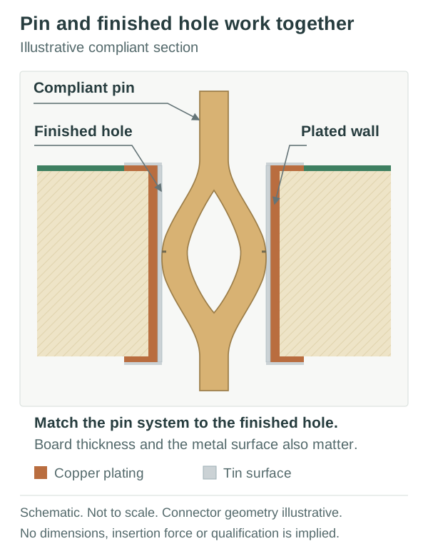
A compliant pin is designed to deform during insertion and establish contact with the plated hole wall. For the selected connector system, FLJ manufactures the finished-hole geometry, copper plating and tin-covered contact surface together. Board thickness and the pin’s contact section must also provide the intended engagement.
For mixed SMT and through-hole builds, we coordinate later connector installation and soldering with the fitted components, access and board support. The sequence also accounts for the heat received by tin-finished areas awaiting their final connection.
Tin Thickness and Solderability
FLJ coordinates the tin finish, protective packing and assembly sequence to keep the surface useful through the last planned soldering operation.
Total Tin, Free Tin and the Copper–Tin Interface
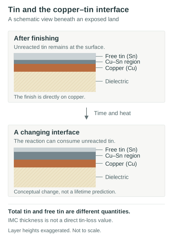
The deposited finish begins with metallic tin at the copper surface. As copper and tin react, part of the tin enters a Cu–Sn intermetallic region. Free tin is the unreacted metallic tin that remains. A total-tin measurement accounts for tin on its defined measurement basis, including tin that may already be in the reaction region; it does not identify the unreacted portion by itself.
A total-tin result alone therefore does not establish the remaining free tin. The physical thickness of the intermetallic region is a different quantity, rather than a direct tin-loss value to subtract from that result.
As-finished tin coating: approximately 1 µm as a typical thickness scale. This describes the initial deposited coating, before its later storage and assembly history. The build specification sets the required thickness and the measurement method and timing.
Keeping the Finish Ready for Assembly
FLJ packs finished boards to limit surface contact and rubbing, then carries the finish requirements into the assembly plan. Clean handling and coordinated storage, reflow and later soldering help retain a usable surface at the final connection.
Packaging protects against contamination and handling, while the copper–tin interface continues to change with its time and temperature history. Tin-whisker mitigation is addressed through deposit structure, process control and qualification appropriate to the application.
Request Immersion Tin PCB Manufacturing
Send your board files, quantity, tin-finish requirements and assembly scope. FLJ supplies finished bare boards or fabrication with component assembly.