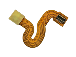
Flex PCB Bend Radius: Static vs Dynamic Designs and the Assembly Handoff
Specify the actual flex path, bend duty, stackup and assembly sequence instead of relying on a generic radius multiplier for every design.

PCB manufacturing & turnkey assembly · Shenzhen, China
FLJ PCBManufacturing your next ideaFLJ resources
PCB design and layout guides covering stackups, vias, material choices, fabrication checks and assembly handoff. Select a topic to review the design constraints and release information relevant to your board.
Showing 1–12 of 37 articles

Specify the actual flex path, bend duty, stackup and assembly sequence instead of relying on a generic radius multiplier for every design.

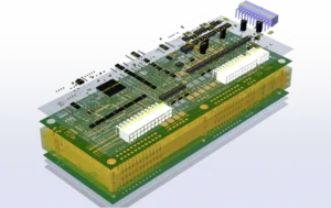
Large language models are beginning to change PCB design by helping engineers interpret requirements, work with EDA data, and operate design software. They are not yet a substitute…

A PCB manufacturer normally needs four things to prepare an accurate quote: complete manufacturing data, the board’s technical specifications, the required quantity, and delivery or compliance requirements. For…

Most PCBs are green because a green solder mask covers their outer copper layers. The solder mask, also called solder resist, is a protective insulating coating applied during…

A multilayer PCB rarely fails because one production step was “bad.” More often, the layout, stack-up, drill strategy, and inspection plan were not aligned before fabrication began. Once…

1. Via Design in High-Speed PCBs In high-speed PCB design, multilayer PCBs are often required. Vias are an important part of multilayer PCB design. A PCB via mainly…

When PCB Materials Fail: The Cost of Ignoring IPC-4101 In 2019, a Tier-1 automotive supplier recalled 40,000 engine control units. The root cause was not a component defect.…

Introduction: Why Thermal Management Matters in LED Lighting LED lighting has transformed how we illuminate homes, businesses, and public spaces, offering superior energy efficiency and longevity compared to…

1. Process Background As PCBA components become smaller and more dense, the distance between parts and the stand-off height of parts, which is the gap between the part…

What Is a Ceramic PCB? A ceramic PCB uses an inorganic ceramic substrate instead of traditional FR‑4 fiberglass. Common substrate materials are alumina (Al₂O₃), aluminum nitride (AlN), and beryllium oxide (BeO). These boards conduct heat…

When we take on a project that is outside our comfort zone, we have all been there at one time or another. For me, that day came when…

In simple terms, silkscreen is the non conductive legend printed on the board to identify components, pin 1, polarity, connectors, jumpers, test points, warnings, logos, revision codes. All…