
STACKUP ENGINEERING · PRECISION FABRICATION · TDR
Controlled Impedance
PCB Manufacturing
The electrical target.
The construction to achieve it.
FLJ provides stackup development, single-ended and differential impedance calculations, controlled-impedance fabrication and TDR verification. Material selection, finished trace geometry and test structures are developed around the board’s electrical requirements, from prototype to production.
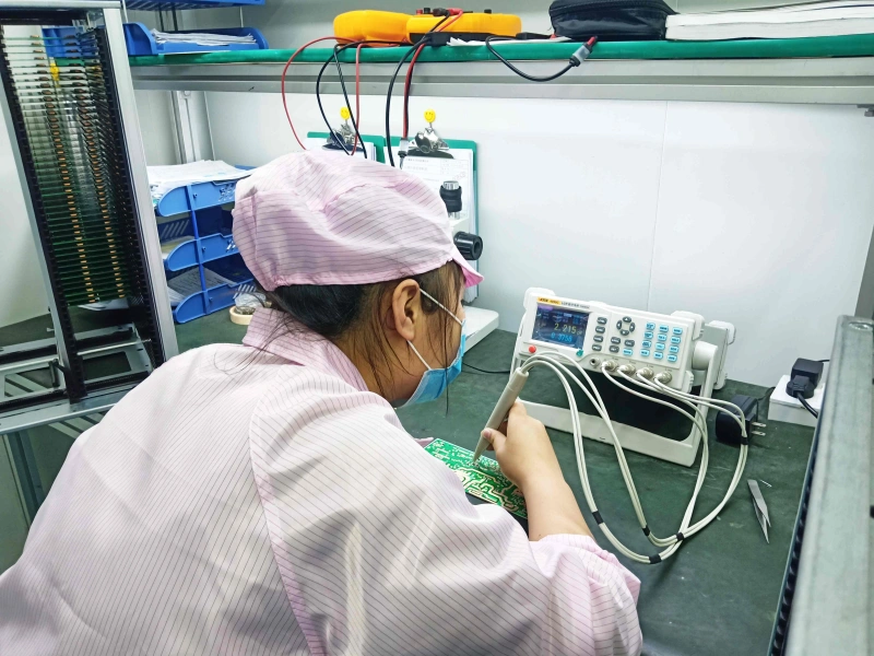
ENGINEERING, BOARD FABRICATION AND VERIFICATION
Controlled Impedance PCB Services
The service covers the engineering definition and the manufactured board. Work can begin with an electrical target for a new design or with an existing layout and stackup.
Stackup development
FLJ develops the layer arrangement, laminate and bonding construction around the board’s mechanical and electrical needs. An existing multilayer stackup can also be evaluated using the relevant material and process dimensions.
Impedance calculations
Single-ended and differential line models connect the target impedance to conductor width, copper thickness, reference spacing and pair gap. The calculation establishes a coordinated geometry for the selected layer and transmission-line structure.
Material and construction selection
Core, prepreg, copper weight and foil-built or core-built construction are selected together. Conventional FR-4, low-loss materials and compatible mixed-material buildups provide options for the circuit’s electrical role.
Controlled-impedance fabrication
Manufacturing forms the pressed dielectric, finished copper profile and layer connections described by the engineering construction. Imaging, etching, lamination and plating contribute to those physical dimensions.
TDR testing and documentation
Representative coupons provide defined structures for impedance measurement. Results are recorded with their target, tolerance and relevant production identification, connecting the measurement to the board construction.
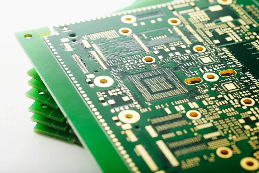
SIGNAL BEHAVIOR STARTS WITH THE PHYSICAL PATH
Why Controlled Impedance Matters
A transmission line includes the signal conductor, its reference conductors and the dielectric between them.
That arrangement distributes inductance and capacitance along the route, giving the line its characteristic impedance. A change in conductor geometry or reference structure can create a discontinuity. Part of the travelling signal is then reflected, changing the waveform that reaches the receiver.
A trace widening into a pad changes its local capacitance; a change in reference spacing alters the line’s field geometry. The reflected component can return while another transition is propagating, modifying the voltage seen along the path. These are physical reasons to keep the intended conductor and reference structure consistent.
On fast digital connections, reflections can consume noise and timing margin. On an RF path, discontinuities disturb the intended transmission environment. Controlled manufacture addresses the trace and dielectric dimensions that contribute to these effects.
Transition speed, propagation distance and the circuit’s requirements determine where control is useful. A clock-frequency label alone does not describe that relationship. FLJ combines the required line geometry with the wider construction of high-speed digital boards and RF and microwave circuits.
FROM THE LINE MODEL TO FINISHED COPPER
How FLJ Controls PCB Impedance
The target, transmission-line model and fabrication geometry describe one structure. Engineering develops that structure using dimensions and material properties appropriate to the finished board.
Microstrip
A surface trace runs over a reference plane. The model includes its width and copper profile, the dielectric separation and the environment above the trace, including the selected solder mask.
Stripline
An internal trace lies between reference conductors. The material and spacing on each side form part of the model; an asymmetric construction uses the corresponding unequal separations.
Grounded coplanar
Ground copper beside the signal joins the reference structure below. Lateral ground clearance is an additional dimension alongside trace width and vertical dielectric spacing.
Illustrative sections, not to scale. Single-ended and differential operation are signal modes that can be implemented in these structures.
Develop the stackup and line together
FLJ combines the selected laminate system and dielectric data with the expected pressed layer separations. Material Dk is used in its applicable construction and measurement context. A material family name alone does not define the electrical geometry.
Prepreg contains glass reinforcement and partly cured resin. During lamination, resin flows around the copper pattern and cures into the bonded structure. Its incoming designation therefore does not, on its own, specify the final local distance between a trace and its reference plane.
The model uses the finished copper thickness and conductor profile along with that separation. For a differential pair, the gap between the two traces enters the coupled structure. A 100 Ω differential target refers to the pair under differential excitation, rather than a 100 Ω target applied independently to each line.
With a fixed stackup, the model establishes finished width and pair spacing for that construction. When component escape or routing pitch limits those dimensions, the dielectric buildup and reference arrangement provide other engineering choices. The dimensions are solved together, keeping the target tied to a buildable structure.
FLJ records the selected stackup and calculated line dimensions for fabrication. Proposed changes to an existing layout’s width or spacing are documented before production, so the engineering geometry and manufacturing data describe the same line.
Control the dimensions in production
Imaging and etching. Artwork compensation accounts for the expected transfer and etching result. Finished line width and sidewall shape belong to the conductor cross-section used in the model.
Lamination. Prepreg selection, copper distribution and the press cycle affect resin fill and the cured dielectric arrangement. Layer registration holds conductors and references in the intended relationship.
Copper and coating. Foil and applicable plating operations build the finished copper thickness. An outer-layer model includes the selected solder-mask structure around the trace.
Physical checks. Dimensional inspection and selected cross-sections examine the manufactured geometry. TDR measurements address the electrical behavior of the corresponding test structure.
| Parameter | Physical object | Engineering and production work |
|---|---|---|
| Reference spacing | Local dielectric between signal and reference conductors | Core/prepreg selection and the pressed construction used in the model |
| Conductor width and thickness | Finished copper cross-section, including its sidewalls | Imaging, etch compensation and the applicable copper build |
| Pair or ground gap | Spacing to the other signal or adjacent coplanar ground | Coupled-line modeling and control of the finished separation |
| Dielectric environment | Selected laminate and relevant outer coating | Material data and the corresponding coated or uncoated line model |
A PRACTICAL STACKUP DECISION
Foil-Built vs. Core-Built PCB Construction
Both routes can produce an impedance-controlled multilayer board. The difference is how the copper and dielectric layers are assembled, including the construction beside the outer traces.
Foil-built
Four-layer exampleOuter copper begins as foil bonded into the stack with prepreg. In this example, the outer traces reference inner copper across a pressed prepreg layer. The internal core carries the central copper pair.
Core-built
Four-layer exampleCopper-clad cores form the outer portions of the stack. The illustrated outer trace and its reference are separated by cured core dielectric. Prepreg bonds the core sections together.
Illustrative constructions, not released stackups or thickness specifications.
| Consideration | Foil-built | Core-built |
|---|---|---|
| Outer copper | Selected copper foil is incorporated into the buildup. | Outer copper begins on the selected copper-clad core. |
| Illustrated outer reference spacing | Based on the expected pressed prepreg thickness. | Based on the relevant cured core dielectric thickness. |
| Copper-weight combinations | Foil selection can provide the required outer copper independently of a special outer-core pairing. | The required copper combination must be available on the selected core, or addressed by the fabrication route. |
| Processing and cost | Depends on foil, internal cores, bonding materials and the complete buildup. | Depends on core specifications, availability and any additional processing needed for the copper arrangement. |
For a thin outer signal-to-reference separation, the illustrated foil-built route places that spacing in a pressed bonding layer; the core-built route requires the corresponding cured core thickness. The available dielectric and copper combinations therefore influence which construction fits the intended line geometry.
A selected foil weight can avoid sourcing a special outer core with that copper combination. Conversely, a core whose thickness and copper faces already match the intended construction can provide a practical core-built route. FLJ compares these combinations with the compatible bonding system and the complete buildup, including any additional copper processing.
FLJ selects the route together with the impedance geometry and overall board thickness. The comparison concerns the complete construction and its processing, rather than a fixed price difference between the two names. Each route uses its corresponding material and finished-dimension inputs in the model.
MEASURE A DEFINED STRUCTURE. REPORT A DEFINED RESULT.
TDR Impedance Testing and Reports
FLJ uses representative impedance coupons manufactured with the relevant production panel and stackup. Their line geometry, layer references and coating condition correspond to the structures being verified.
From coupon to measurement
Time-domain reflectometry applies a fast transition and interprets the reflected response. A defined coupon gives the measurement a consistent conductor structure and test connection. Single-ended and differential targets use the appropriate model and measurement configuration.
The instrument, cables, probes and connection to the coupon form the measurement setup. Calibration establishes the applicable reference, and the region used for the line value is chosen to represent the coupon trace. Contact, launch and end responses are recognized in the setup and interpretation.
Separate layer or signal-mode structures retain their corresponding identifiers, targets and results in the report. Each reading can then be evaluated against the tolerance for that structure.
Actual routed channels may contain vias, connector launches and reference changes. Their behavior can also be investigated with suitable measurement access and interpretation. A uniform coupon result describes the represented fabrication structure; evaluation of the complete routed or assembled channel addresses a wider object.
Bare-board electrical testing separately checks continuity and isolation. These network checks complement impedance verification.
READING THE DELIVERABLE
What the impedance report identifies
- Target and tolerance
- The specified electrical value and its acceptance interval.
- Structure and mode
- Coupon identification, layer/reference arrangement and single-ended or differential definition.
- Measured result
- The result associated with that defined test structure and method.
- Production reference
- Identification connecting the sample and record to the relevant build and stackup.
Acceptance arithmetic example; not a measured FLJ test result.
Fabrication tolerance reference
For the defined stackup and target, the published FLJ fabrication reference is ±5 Ω below 50 Ω and ±10% at 50 Ω or above. This is the impedance acceptance reference, distinct from the instrument’s measurement uncertainty.
PRACTICAL ENGINEERING QUESTIONS
Controlled Impedance PCB FAQs
Does every PCB need controlled impedance?
The need depends on signal transitions, propagation distance and the circuit’s requirements. Fast digital interconnects and RF paths are common applications. The relevant device and interface requirements identify which structures need a target, rather than applying one clock-frequency threshold to every board.
Why can the fabrication trace width differ from the initial EDA calculation?
The fabrication model uses the selected material and expected finished geometry. Pressed dielectric separation, copper thickness, conductor shape and outer coating can differ from a calculator’s initial assumptions. FLJ develops the corresponding width or spacing and documents proposed changes to an existing layout before production.
Is controlled dielectric the same as controlled impedance?
A controlled-dielectric construction specifies dielectric and copper dimensions. An impedance-controlled build defines an electrical target for selected line structures and uses the associated geometry control and verification. FLJ can work from a supplied stackup or develop a construction around the impedance target.
What should be included in a controlled-impedance PCB enquiry?
Send the fabrication files and available stackup, with the target impedance, tolerance, signal mode and applicable layers or structure identifiers. Include quantity and any material constraints. Add the BOM and placement data when PCB assembly is part of the delivery.
Engineering support, bare-board fabrication and optional assembly for prototypes and production.
Send your project to FLJ →