
High-Tg PCB
Manufacturing
Build thermal performance into the board.
FLJ manufactures high-Tg printed circuit boards for assemblies exposed to soldering heat and demanding thermal conditions. Material selection, multilayer lamination and plated-hole fabrication work together to produce the finished circuit.
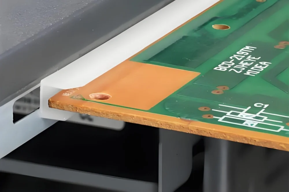
High-Tg PCB Fabrication Capabilities
High-Tg material can be used in a straightforward rigid board or a more complex multilayer construction. FLJ supplies the copper circuitry, interconnections and finished board features as one fabrication service.
Multilayer circuits
High-Tg FR-4 cores and bonding layers support internal routing and reference planes, with dielectric spacing and copper selected for the circuit.
Multilayer PCB fabrication →Dense interconnections
Conventional plated through-holes, blind and buried connections, or suitable HDI buildups connect the layers needed by the layout.
HDI PCB options →Finished-board features
Inner and outer copper, solder mask, exposed-pad finish, routed profiles and panel formats complete the board for its later assembly.
Manufacturing capabilities →Material grade · layer construction · finished thickness · copper by layer · hole and via structures · surface finish · individual boards or panels
Materials and Stackups for the Build
High-Tg FR-4 uses a resin system with a higher glass transition temperature than conventional general-purpose grades. For a Tg170 or Tg180 request, the named laminate and its compatible prepreg define the material system used for the multilayer build. The grade supplies the thermal and electrical properties behind that ordering description.
Tg describes a change in resin behavior, rather than a continuous operating-temperature rating. Decomposition resistance, thickness-direction expansion and the intended soldering exposure also matter to the construction.
FR-4 material and product options →Turn a material choice into a stackup
The core, glass fabric, resin content and copper distribution affect the pressed dielectric construction. Matching those elements produces the spacing, bonded interfaces and finished thickness needed by the board.
A high-Tg choice can coexist with controlled impedance or higher copper weight. Electrical loss, heat removal and thermal durability remain distinct design considerations.
How We Manufacture High-Tg PCBs
The board moves through a complete fabrication route. Within that route, the selected resin system and physical construction guide the lamination, hole preparation and metallization processes.
- Inner circuit
- Lamination
- Drilling & desmear
- Hole copper
- Outer circuit & finish
- Test & delivery
Form the copper before it is enclosed
Imaging and etching create the internal traces, planes, pads and copper clearances. Inner-layer AOI checks the visible pattern before lamination closes access to those surfaces.
Registration brings those patterns into the intended relationship with the later drilled holes. A plated hole must meet the copper pads belonging to its net while retaining clearance from the other copper layers.
Bond the selected material system
The prepared cores, prepreg and outer copper are stacked in the required sequence. Surface preparation promotes bonding at the internal interfaces. Heat and pressure allow the prepreg resin to fill around etched copper features and cure into a bonded insulating layer. Resin flow, pressure and the stack construction work together to maintain layer separation and the intended pressed geometry.
FLJ sets lamination conditions for the chosen material and buildup. Resin content, the surrounding copper and the required dielectric thickness are considered together. Constructions with buried connections or HDI build-up layers introduce the appropriate subassembly and sequential lamination stages.

Create the opening. Prepare the connection.
Drilling establishes the openings through the laminate and its copper layers. Tool condition, drilling settings and board support are matched to the material, thickness and hole geometry to control the resulting hole.
Edge burrs and internal resin smear are different manufacturing objects. Removing copper or glass burrs at an opening does not by itself clean the inner-layer copper contacts inside the hole.
Resin residue can cover the copper that the next metal layer must join. Desmear removes that residue and prepares the exposed resin, glass and copper surfaces for metallization. Wet chemistry, plasma treatment or an appropriate combination follows the selected material and hole construction.
Preparation has to reach the hole interior
A deep, narrow hole presents different treatment conditions at its entrances and its center. Reactive material is consumed and reaction products must leave the hole. A clean-looking opening therefore does not describe the condition of every internal copper contact.
Process control addresses the treatment through the hole, balancing residue removal with preservation of the intended resin and copper interface. Desmear and a specified etchback are different degrees of preparation; removing more material is not automatically a better result.
Turn a nonconductive wall into a copper connection
The drilled wall contains insulating resin and glass. In an electroless-copper route, chemical deposition establishes a thin conductive starting layer over the prepared wall. Electrolytic copper plating then builds the required copper structure.
Copper deposited against the exposed inner-layer pads makes those contacts part of the through-board connection. The prepared interface and the continuous wall copper work together; plating thickness alone does not describe the quality of that contact. This is hole metallization; the later surface finish on exposed soldering pads serves a different purpose.

Complete the finished board
Outer-layer imaging, plating and etching form the surface circuitry through the selected process route. Solder mask protects the intended areas while leaving pads and contacts accessible. ENIG, lead-free HASL, OSP or another suitable finish prepares exposed copper for its later use. Routing, slots and panel separation features complete the mechanical form.
Inspection and Verification of the Manufactured Board
The visible copper pattern, the internal plated connection and the electrical network need different checks. Inspection follows the fabrication work, rather than relying on the laminate’s Tg label to establish the finished result.
| Object | Method or stage | What it addresses |
|---|---|---|
| Inner copper pattern | Inner-layer AOI before lamination | Missing or unwanted copper, bridges and other visible pattern differences. |
| Hole wall & internal connection | Microsection of the relevant specimen | A local view of the plated copper, inner-layer contact and surrounding laminate. |
| Electrical network | Bare-board electrical testing | Required connections and isolation against the fabrication net data. |
| Finished geometry | Dimensional and flatness checks | Board profile, thickness, hole geometry and physical fit. |
| Specified impedance or thermal performance | Appropriate coupons, measurements or thermal-stress evaluation | The defined characteristic of the representative structure or test specimen. |
A microsection examines a local cut through the construction. An electrical test checks the network at the time of testing. A thermal evaluation introduces its specified exposure. Material data describe the laminate, while these checks examine the fabricated board or its representative test structure. Their results complement one another; a successful continuity test alone does not establish long-term thermal life.
Explore PCB testing and inspection →High-Tg Boards, Supplied for the Next Stage
Industrial controls, power conversion and communication hardware can combine dense circuitry with repeated assembly heating or changing operating temperatures. The material and board construction are selected around that actual use.
Prototype fabrication
Build the intended construction early enough to evaluate the physical board, its connections and its assembly fit. Material identity and the selected stackup remain part of that prototype.
Production supply
Manufacturing records connect the material grade, buildup and fabrication route to the boards supplied. This supports consistent repeat builds and makes a material or construction change visible.
PCB assembly
FLJ can continue with component sourcing, SMT and through-hole assembly. The board’s material and construction carry into the assembly plan, while the soldering profile also follows the components and solder system.
PCB assembly services →Start your high-Tg PCB build.
Send the board files, quantity and target date. Include a specified material grade or the available stackup, thickness, copper and connection details. Add the BOM and placement data when assembly is part of the order.