
High-Frequency PCB Manufacturing
From low-loss laminate to finished circuit.
FLJ manufactures high-frequency PCBs using PTFE-based and hydrocarbon ceramic laminates. Choose double-sided, multilayer or hybrid constructions for wireless, sensing and communication electronics, with prototype fabrication, production and PCB assembly from one supplier.

High-Frequency Boards and Material Options
A high-frequency PCB combines a suitable dielectric with copper circuitry that carries the RF signal. Material choice affects the transmission line, the thermal behavior of the board and the way it is fabricated. FLJ supplies the finished circuit, including its plated connections, protective mask, surface finish and profile.
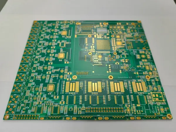
Low-loss boards for demanding RF paths
PTFE-based materials suit circuits where dielectric loss and stable electrical properties are important. Ceramic-filled grades offer additional choices in dielectric constant and thermal behavior. RO3003 is one example within this material group.
Double-sided RF boards and multilayer constructions combine the selected laminate with the copper pattern, plated holes and finished contacts needed by the circuit.
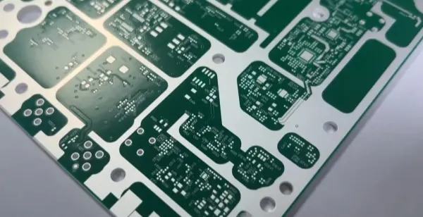
High-frequency circuits in multilayer builds
Hydrocarbon ceramic laminates combine high-frequency electrical properties with processing routes suited to many multilayer designs. Familiar examples include RO4003C and RO4350B.
These materials support boards that bring RF circuitry together with power, control and interconnections, including compatible hybrid constructions.
Manufacturing High-Frequency PCBs
The laminate influences drilling, surface preparation and bonding as well as electrical performance. Our fabrication work follows the selected material system through circuit formation, layer bonding and hole metallization.
Prepare the substrate. Build the copper connection.
Material preparation starts with the selected laminate, copper foil and bonding layers. Panel handling and cleaning protect thin copper features and the surfaces that will form the laminated interfaces.
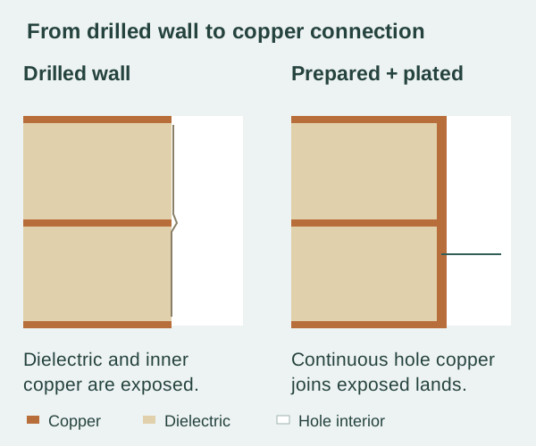
Drilling exposes the dielectric and the edges of internal copper layers along the hole wall. Debris and resin covering those copper edges have to be removed before metallization can form the intended connection. Cleaning and conditioning are selected for the laminate, including the different materials encountered inside a hybrid board.
PTFE has a low-energy surface that needs appropriate activation for copper adhesion. Material-specific preparation makes that surface receptive to metallization. An electroless copper seed can then provide conductivity for electroplating, which builds the hole-wall copper and joins it to the exposed copper lands. Hydrocarbon ceramic grades follow the preparation route specified for their resin system.
Form the copper pattern
Image transfer defines the circuitry, and etching removes the unwanted copper. Production artwork compensation accounts for the way the selected copper thickness and etching process form the finished conductor.
For RF features, the finished line width, gap and copper thickness are part of the electrical geometry. Inspection looks at those physical features as well as breaks, unwanted copper and bridges between adjacent conductors.
The copper surface also matters. A low-profile foil can reduce the contribution of surface roughness to conductor loss, while its treated side still has to bond to the dielectric. Foil selection and surface preparation therefore belong together in the manufactured circuit.
Bond the material into one board
Multilayer fabrication aligns the patterned cores and bonds them with selected prepregs or bonding films. The press cycle follows that bonding system: it develops contact between the layers, allows the applicable flow and cure or bonding stages, and consolidates the stack around its copper features.
Copper distribution influences the space that bonding material must fill. Registration keeps internal pads aligned with the later drilled connections, while the pressed dielectric spacing becomes part of the finished electrical structure. These are physical results of lamination, rather than simply the starting thicknesses listed for the raw materials.
Complete the exposed surfaces
Solder mask protects covered areas while defined openings leave pads and other features exposed. Surface finishing prepares those exposed copper areas for soldering or contact use. Routing, slots and board-edge details complete the shape for the next assembly stage.
Where transmission lines remain exposed, the selected finish can cover RF conductors as well as solder pads. Its metal system and the surrounding mask openings belong to the finished circuit geometry; the choice is made with the line structure and assembly needs in view.
All-High-Frequency and Hybrid Constructions
The same material family can be used in different board constructions. The choice depends on which parts of the circuit need its electrical properties and how the complete assembly will be built.
A dedicated material system
High-frequency cores and compatible bonding layers form the multilayer structure. This gives the circuit designer a material system for RF routing across multiple layers.
Different functions in one board
Selected high-frequency layers carry RF circuitry, while other laminate layers accommodate control, power and additional routing. The bonding system joins these materials into a single manufactured board.

A mixed-material stack brings different expansion and dimensional behavior into one press cycle. Compatible bonding layers, balanced construction and the selected process accommodate those differences. The resulting dielectric spacing and the reference beside the RF path are defined within the complete stack, not by the high-frequency core alone.
Applications for High-Frequency Boards
FLJ fabricates high-frequency boards for communication and sensing electronics, from compact RF circuits to mixed-function assemblies.
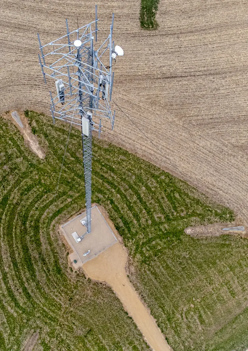
Wireless & communication hardware
RF front ends, antenna circuits and radio links use high-frequency laminates where dielectric loss, dimensional stability and the transmission-line structure matter.
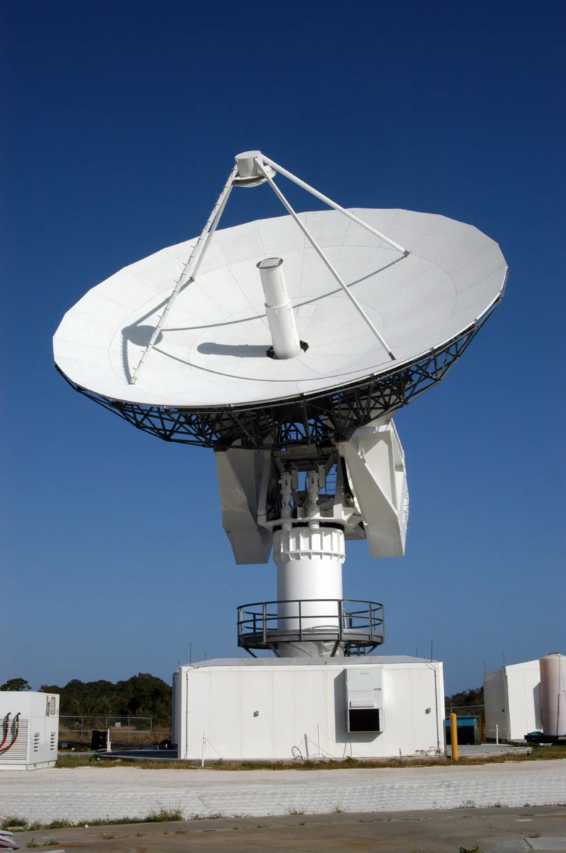
Radar & sensing electronics
High-frequency circuits support radar and sensor functions. Board fabrication combines the selected material with defined conductor patterns, connections and exposed RF features.
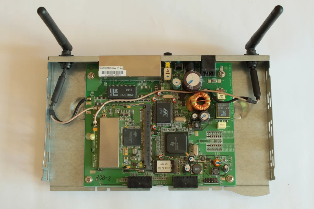
RF and control on the same board
Hybrid multilayers bring the RF section together with control and power circuitry. The material combination follows the electrical role of each part of the construction.
Application reference photographs.
Finished-Board Quality and Production Supply
Inspection follows the objects made during fabrication: copper features, plated connections, laminated interfaces and the final board profile.
Copper & circuit continuity
Optical inspection checks the circuit pattern. Electrical testing checks opens and shorts against the board data.
Holes & internal structure
Microsection inspection can show local hole-wall copper and internal layer connections. It adds a view inside the board that surface inspection cannot provide.
Defined electrical features
Controlled-impedance features can be verified using suitable test coupons. RF loss or other frequency-domain measurements need the corresponding test structures and measurement scope.
Start your high-frequency PCB build.
Order the bare board or combine fabrication with component sourcing and PCB assembly. For the move from prototype to production, the laminate grade, foil and stackup remain defined parts of the build. Any material or construction change is reviewed for its effect on fabrication and the circuit before it is introduced.
Can high-frequency material be combined with FR-4?
Yes. Compatible hybrid constructions combine selected high-frequency material with FR-4 layers. Laminate properties, bonding materials and the fabrication sequence are considered together when developing the stack.
Can FLJ supply assembled high-frequency boards?
Yes. PCB assembly can be combined with bare-board fabrication and component sourcing, covering the board and its populated assembly in one supply route.