
PCB FABRICATION + COMPONENT ASSEMBLY
Aerospace PCB
Manufacturing
& Assembly
Bare-board fabrication and complete PCB assemblies for aerospace electronics.
FLJ manufactures multilayer rigid, HDI and rigid-flex PCBs and assembles the components, connectors and interfaces specified for your aerospace electronics. Source bare boards, a turnkey build or assembly with your supplied components.
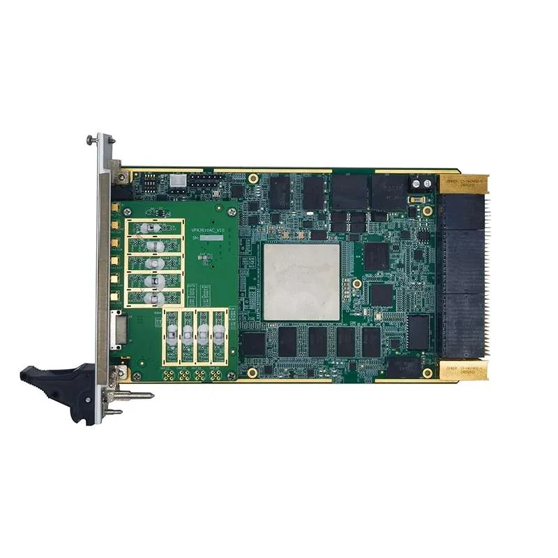
Aerospace PCB Constructions and Materials
FLJ manufactures multilayer rigid, HDI, flexible and rigid-flex PCBs for aerospace electronics, with bare-board supply and component assembly. Construction selection brings the circuit’s routing density, signal requirements and equipment packaging into the same stack-up.
Flexible and Rigid-Flex Interconnections
Flexible circuits connect separated or space-constrained component regions. In a rigid-flex PCB, routed rigid layers and PI-film interconnects form one board construction. Bend location, installed shape, coverlay openings and the rigid-to-flex transition determine how the circuit fits the equipment. A supported connector or component region remains mechanically different from the flexible span.

RF and Mixed-Material Constructions
A low-loss RF laminate can carry the radio-frequency path while compatible control and power layers form the rest of a hybrid stack-up. Bonding materials, copper thickness and layer references must suit that combination. Operating band, dielectric data and trace geometry are considered together: dielectric values belong to a defined material construction and test frequency.
Aerospace PCB Fabrication Capabilities
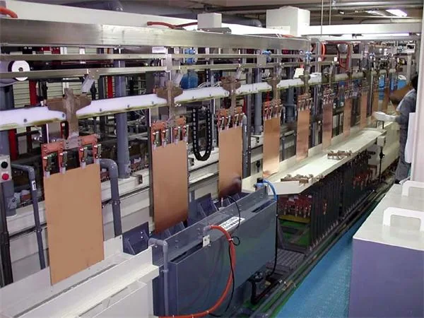
FLJ produces the copper patterns, laminated structure and plated interconnects that turn the specified stack-up into a finished board. Inner-layer processing, lamination, hole preparation and copper deposition each establish geometry needed by the next operation.
Stack-Up, Lamination and Layer Registration
Inner copper is imaged and etched on cured copper-clad cores, then inspected before it is enclosed. Bonding preparation and layer registration establish the relationship between those patterns and the later drill locations. Dimensional compensation accounts for measured core expansion or shrinkage, helping preserve the intended capture-pad connection around each hole.
New prepreg supplies resin to fill the spaces around the copper pattern and bond the stack. Its glass style, resin content and flow must fit the copper relief and required pressed thickness. The press cycle establishes both the layer bond and the dielectric spacing used by the impedance model; an unpressed sheet designation alone does not define that spacing.
Drilling, Via Filling and Plated Interconnects
Mechanical drilling opens the path through the laminated stack. Drill selection, chip evacuation and hole-wall preparation follow the board material, depth and hole size. Desmear removes drilling residue to expose the inner-layer copper. Metallization establishes a conductive surface on the insulating wall, and electroplating builds the copper connection. Copper distribution inside the hole is controlled alongside the copper deposited on the panel surface.
HDI builds use laser openings to reach specified target lands. Hole-bottom cleaning and copper filling prepare the connection for its intended build-up. A resin-filled through-hole with a copper cap is a different construction from a copper-filled microvia; the required fill, cap and landing surface are specified separately. Our microvia fabrication options explain the layer arrangements and interfaces.
Copper Geometry and Impedance Control
Imaging, etching and plating establish the finished copper profile; lamination establishes its distance to the reference plane. FLJ coordinates those dimensions with the material model for controlled-impedance fabrication and TDR testing. The published fabrication reference is ±5 Ω for targets below 50 Ω and ±10% for targets of 50 Ω or higher.
The construction references below support an initial manufacturing discussion. Each limit applies to its named feature; layer count, copper, hole size and clearances are combined into the quoted stack-up.
Fabrication references by board construction
Scroll horizontally to view all columns.
| Reference capability | Multilayer rigid | HDI | Rigid-flex |
|---|---|---|---|
| Maximum layer count | 30 | 24 | 16 |
| Maximum finished copper per layer | 6 oz | 2 oz | 2 oz |
| Minimum mechanical drill diameter | 0.15 mm | 0.127 mm | 0.15 mm |
| Through-hole aspect ratio | Up to 10:1 | Up to 10:1 | Up to 10:1 |
| Laser microvia drill / paired pad references | 4 mil / 10 mil (101.6 / 254 µm); 5 mil / 11 mil (127 / 279.4 µm) | ||
Finished thickness and line width/spacing follow the chosen stack-up and copper build. Mechanical drill diameter is the tool dimension; plating reduces the finished hole opening. The laser-hole/pad pairings describe microvia geometry. Explore the manufacturing capability categories for related processes.
Aerospace PCB Assembly Services
FLJ supplies aerospace PCB assembly as a complete turnkey build, a partial-sourcing build, or assembly with customer-consigned components. Procurement scope follows the released BOM and the parts supplied by the customer, so the quote identifies which components FLJ will source and which will arrive on consignment.
Component Procurement and Approved Alternatives
FLJ’s component procurement service can quote the specified BOM and propose alternative brands or parts when availability, lead time or cost changes. Engineering comparisons cover the complete manufacturer part number, package, pin assignment, electrical requirements and temperature grade alongside the commercial options. The selected alternative enters the approved BOM before it is released for the build.
This gives procurement a defined choice between the original BOM, an approved alternative-parts quotation and a combination of sourced and consigned components.
SMT, Through-Hole and Connector Assembly
FLJ combines SMT placement with through-hole soldering and connector attachment for mixed-technology boards. Component thermal mass, board construction and attachment method guide the soldering sequence and profile. Support tooling holds the assembly through the applicable operations, while connector mounting includes the soldered joint and the required mechanical attachment.
The supplied assembly can include dense processing circuitry, larger power parts and board-edge interfaces. Required test contacts and connector mating areas remain accessible for the subsequent checks and final equipment connection.

Cleaning, Coating and Functional Test
Cleaning prepares the designated surfaces for the selected conformal coating process. Masking keeps mating contacts, test points and other specified areas clear; application and cure follow the coating material and assembly requirements. This protection is selected for the surface environment of the equipment.
Programming and board-level functional testing use the released firmware, defined supply, inputs, outputs and load. The test procedure establishes the expected responses and pass criteria, so results identify the board function checked under those conditions.
Request a PCB Assembly QuotationBare-board and assembly scope can be quoted together.
Applications in Aircraft and Space Electronics
Aerospace equipment combines processing and interfaces, RF signal paths, and power electronics. The board construction and assembly work follow the role of each circuit within that equipment.
Avionics and Aircraft Instrumentation
Instrumentation boards receive sensor and control inputs, then route signals to displays or other aircraft electronics. Mixed analog and digital circuitry needs considered routing, grounding and connector placement. Multilayer rigid boards support dense interfaces; rigid-flex can connect assemblies in limited space. Fabrication controls layer registration and plated interconnects, while assembly places interface components and board connectors to the equipment layout.
RF Communication and Satellite Payload Electronics
Communication and payload electronics connect RF front ends, processing circuits and antenna or subsystem interfaces. The signal trace, nearby reference copper and connector launch form a continuous RF path; low-loss materials and controlled geometry support that path through the board. Space payload projects add their specified vacuum/outgassing, thermal and radiation requirements to the material, component and verification plan.
Power Distribution and Equipment Monitoring
Power boards distribute an input supply, switch loads and collect voltage or current measurements. Copper paths, plated connections and terminals are sized around current, voltage, permissible temperature rise and cooling. Component assembly also brings the switching devices, magnetics, sensing circuits and heat-transfer interfaces together. A converter’s power stage and separate control board illustrate the different electrical and assembly tasks within one unit.

Aerospace PCB Inspection and Delivery Documentation
FLJ links the delivered board or assembly to its drawing revision and the ordered inspection records. Material identification, manufacturing observations and electrical results describe different parts of that build, so the record package identifies what was checked and the applicable acceptance criteria.
Bare-Board Inspection and Test Records
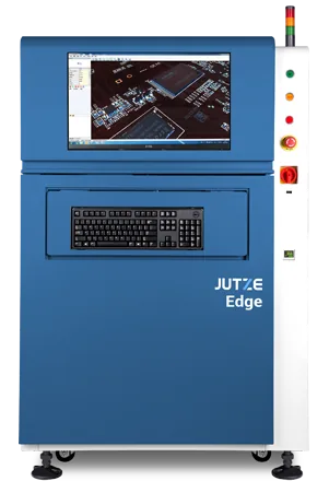
Inner-layer AOI examines the copper pattern before lamination. After fabrication, dimensional inspection and electrical network testing address the completed board. Sections and impedance coupons provide additional evidence about the features they represent.
Checks and records associated with the manufactured board
Scroll horizontally to view all columns.
| Object | Check | Related delivery record |
|---|---|---|
| Laminate and stack-up | Material and layer construction identification | Build revision, stack-up, and material or lot documentation as specified |
| Inner copper pattern | AOI before lamination | Pattern inspection associated with the inner-layer artwork |
| Finished bare-board network | Continuity and isolation test | Net-test results and production-lot identification |
| Impedance coupon | TDR measurement against the ordered target | Coupon identification, layer/reference, test mode, target, and measured result |
| Interconnect sample | Cross-section of specified hole, copper, land, and interface features | Sample location and measured observations against the agreed plan |
Thermal cycling or broader interconnect qualification is performed only when a defined plan, sample, and acceptance criteria are part of the scope.
Assembly Traceability and First-Article Documentation
For assembled product, the delivery records connect the BOM and approved substitutions with component identification, assembly revision and required first-article observations. AOI examines visible component and solder features; X-ray examines selected hidden connections. Ordered process-profile and electrical or functional records identify the assembly and procedure used.
The purchase specification identifies the standard, revision, class and any addendum. IPC-6012 addresses rigid-board performance, IPC-6013 flexible and rigid-flex boards, and IPC-A-600 bare-board acceptability. J-STD-001 and IPC-A-610 address soldering requirements and assembly acceptability. IAQG 9100 concerns the quality management system; product acceptance follows the specified board and assembly criteria.
Aerospace PCB FAQs
Can FLJ supply both bare PCBs and assembled aerospace boards?
Yes. FLJ supplies bare boards and assembled units. For bare-board supply, send fabrication data and the stack-up. For assembly, include the BOM and assembly drawings, plus the required inspections or tests.
How do aircraft and space PCB requirements differ?
Requirements follow the equipment. Aircraft and space systems may differ in temperature, vibration, pressure, radiation, and service life. Specify mission profile and acceptance criteria; radiation and vacuum needs are design-specific.
When should I choose FR-4, polyimide or an RF laminate?
Choose for electrical, thermal, mechanical, and fabrication needs. Reinforced rigid polyimide differs from flexible film. RF designs need material data suited to operating frequency and stack-up.
Which manufacturing and acceptance standards should be specified?
Specify the standard, class, revision, and addenda for each product or process. Quality-system certification does not certify the PCB or assembly. Agree acceptance criteria with the design authority.
What documentation can accompany a first-article delivery?
Agree the record package: material, construction, assembly and component traceability, and required inspection or test records. First-article documents should match the delivered board and acceptance plan.
How are component alternatives handled for an aerospace build?
FLJ can recommend and quote alternatives against the approved BOM. The comparison covers full part numbers, package, pin assignment, electrical requirements and temperature grade. The selected substitution is approved before production and recorded in the build BOM.
What affects the cost and lead time of an aerospace PCB project?
Price and schedule depend on material availability, layer count, sequential lamination, finish, inspection, and assembly components. Send design files, quantity, BOM, required records, and delivery target for a quote.
Bring the board and assembly requirements together.
Send fabrication data and stack-up, quantities, and any assembly BOM and drawings. Include required records, tests and your delivery target so the quotation covers the complete supply.