
PCB Manufacturing Services for Prototype and Production
Custom bare-board fabrication for your next product. FLJ PCB / Philifast in Shenzhen connects board construction, materials, engineering review and inspection—from a first prototype to repeat production.
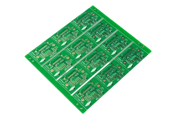
PCB constructions for your product
PCB manufacturing turns your circuit and mechanical design into a bare printed circuit board: copper connections, insulating layers, holes, protective mask and finished soldering or contact surfaces. PCB assembly adds components to that board.
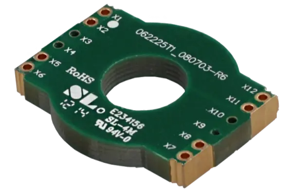
Rigid and multilayer PCB
FR4 constructions for control, power and general electronics, with routing and reference planes matched to the layer stackup.
Explore →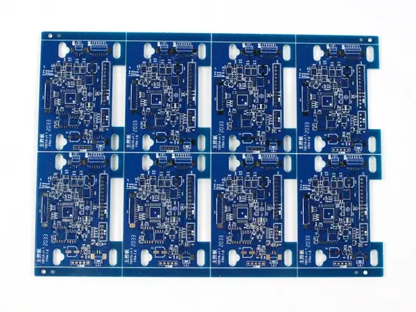
HDI PCB manufacturing
Build-up layers, laser microvias and dense interconnects for compact layouts and fine-pitch component escape.
Explore →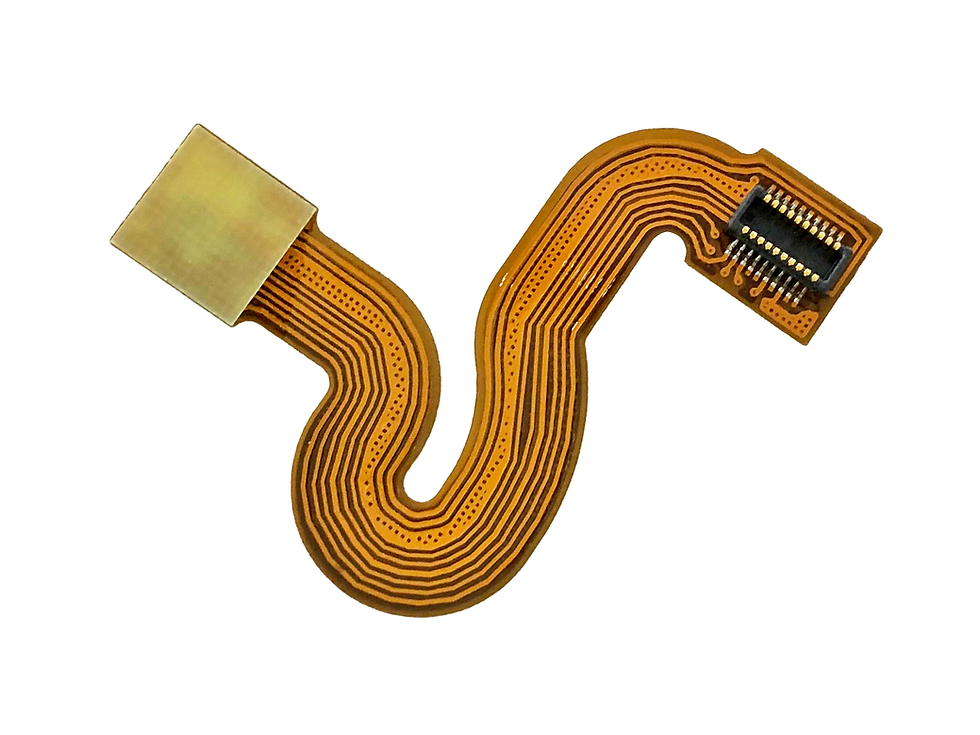
Flexible PCB fabrication
Flexible interconnections with coverlay and local reinforcement for folding, connector fit and compact packaging.
Explore →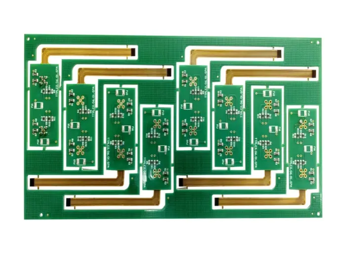
Rigid-flex PCB
Rigid mounting regions and flexible connections combined in one construction; reviewed around the mechanical drawing.
Explore →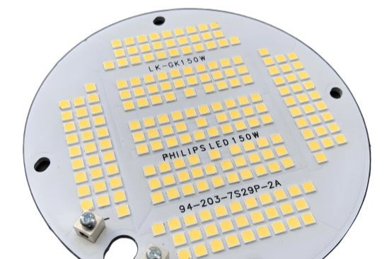
Metal-core PCB
Aluminum and copper-based constructions for a defined thermal path, electrical insulation and mounting arrangement.
Explore →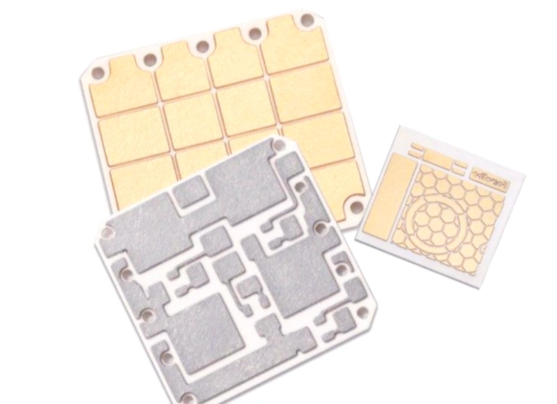
Ceramic PCB
Specialized ceramic substrates for applications where material, metallization and thermal behavior guide the board choice.
Explore →PCB manufacturing capabilities at a glance
Use these selected references to start the discussion. Our engineers match each feature with the material, copper and process route; specialist-board figures describe their own construction.
| Manufacturing choice | FLJ scope / reference | What it means for your build |
|---|---|---|
| General rigid PCB layers | 1–30 layers | Layer count and construction reviewed with your circuit and board drawing |
| Finished copper, general scope | Outer up to 8 oz; inner up to 6 oz | Trace geometry and copper distribution reviewed with copper weight |
| Minimum line / space at 0.5 oz | 3 / 3 mil | Copper-specific reference; heavier copper uses different clearances |
| Mechanical finished-hole range | 0.10–6.2 mm | Finished opening differs from drill diameter; board depth and material matter |
| Maximum finished size, 2–20 layers | 21 × 33 in (533.4 × 838.2 mm) | This layer range; process panels and specialist board sizes are assessed separately |
| Controlled impedance | ±5 Ω below 50 Ω; ±10% at or above 50 Ω | Defined stackup, target and agreed verification |
| Specialist HDI laser-hole reference | 0.075 mm | HDI process scope; dielectric, land and fill reviewed together |
| Surface finish options | ENIG, lead-free HASL, OSP, immersion tin/silver and plated gold | Select around soldering, contacts and the drawing |
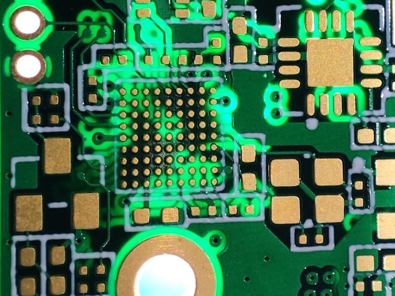
Materials and stackup matched to your circuit
A PCB material choice connects electrical behavior, assembly temperature, insulation, mechanical fit and sourcing. Send a nominated grade or explain the operating needs; we can review options with you.
FLJ’s published material range includes standard and high-Tg FR4, polyimide flex materials, RF laminates and metal-based systems. Examples include Shengyi and Kingboard FR4 grades, Isola FR408/FR408HR, Panasonic Megtron families and Rogers RF laminates. Exact grades and availability are checked for the build.
For controlled impedance PCB fabrication, review the reference planes, dielectric spacing, finished copper and trace geometry together. A nominal prepreg thickness is not necessarily its final pressed thickness. The proposed stackup gives routing and manufacturing a shared reference before production.
For RF and high-speed designs, compare the selected material’s dielectric data at the relevant frequency and test method. For power or thermal designs, connect copper and dielectric choices with the cooling path. A substitute material is discussed with your team before approval.
Prototype, low-volume and repeat production
Choose a manufacturing route around the stage of your product. Quantity is one part of the decision; design maturity, construction, material availability and acceptance also shape the build.
Prototype PCB fabrication
First hardware or a design revisionCheck board fit, circuitry, construction and the details needed for the next revision
Low-volume PCB manufacturing
Small runs or multiple product variantsCoordinate quantities, revisions and material choices without losing build identity
Repeat / volume production
A released design with ongoing demandKeep material, manufacturing revision, test scope and changes connected between orders
Quick-turn PCB fabrication
A date-sensitive board requirementShare the target date; engineering, materials and process route are reviewed before scheduling
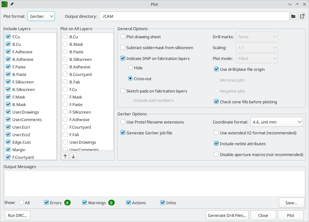
DFM review before fabrication
Design for manufacturing connects your released data with a practical fabrication route. Our engineers review the board files and discuss useful changes or open questions with your team.
A CAD design-rule check tests the rules in your layout environment. A fabrication review also considers the selected manufacturing process. If a detail is still open, send the current files or explain the requirement—we will follow up with the relevant engineering questions.
Changes to materials, holes, copper or the outline are agreed with your team before the manufacturing package is released. Repeat orders use an identified revision, with changes reviewed against the previous build.
Copper and spacing
Finished copper, trace width and clearances
Holes and vias
Finished-hole needs, plated/non-plated features and via spans
Mask and markings
Pad openings, bridges and reference markings
Outline and panel
Slots, edge contacts, V-scoring and breakaway features
Stackup and signal needs
Layer order, material and impedance targets
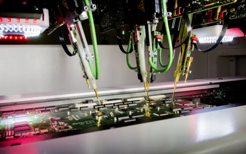
From fabrication data to finished boards
The sequence follows the construction. Multilayer and HDI boards include additional layer-building stages; a straightforward rigid board uses a different route.

- 01
Engineering release
Review artwork, drill information, outline and construction
- 02
Inner layers and inspection
Image and etch inner copper for multilayer boards; inspect the pattern
- 03
Lamination and drilling
Align layers and dielectric, press the stack, then create the specified holes
- 04
Interconnections and outer copper
Apply the selected metallization and copper-pattern processes
- 05
Mask, finish and profiling
Apply mask/legend, finish exposed copper and complete the outline
- 06
Verification and packing
Perform the agreed inspection/electrical checks and protective packing
Advanced features and surface finishes
Dense routing, high current and mechanical interfaces call for different fabrication details. Tell us the function a feature needs to perform, and we will review its construction.
For specialized circuit constructions, explore IC substrate PCBs and embedded PCBs.
HDI and via filling
Microvias, build-up layers and specified via-in-pad arrangements
Heavy copper PCB
Copper-specific line/space and distribution
Controlled impedance / RF
Specified stackup, laminate and geometry
Gold fingers and castellations
Contact finish, bevel or plated edge geometry
Backdrilling and mechanical details
Via stub target, depth-controlled work, slots and profiling
Finish selection
ENIG, HASL, OSP, immersion finishes or plated gold
Inspection and acceptance connected to your board
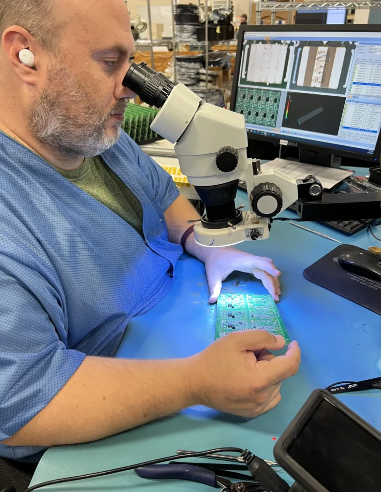
Bare-board electrical testing checks intended connectivity and isolation. It complements dimensional and visual inspection; it does not establish assembled-product function.
Agree the relevant checks with the board specification: copper-pattern inspection, finished dimensions, holes, mask, surface finish and electrical test. Controlled impedance or other specialized verification is defined with its targets, sampling and reporting arrangement.
IPC-A-600 concerns printed-board acceptability, while IPC-6012 addresses qualification and performance for rigid printed boards. Use the applicable document, revision and acceptance class for the actual construction. These technical requirements serve a different purpose from an ISO management-system certificate.
For supplier qualification, our team can discuss current certificates and the relevant entity, site and scope. Material declarations, applicable PCB recognition and any finished-product market approvals are addressed separately.
What affects a PCB fabrication quote?
An accurate PCB quote connects your board configuration with the quantities and delivery you need. Send the present data; we will help resolve the details that affect the manufacturing route.
Board size and panel use
Outline, arrays and usable material
Layer stack and material
Layer count, exact grade and dielectric construction
Copper, holes and feature density
Copper weight, small features, via types and filling
Finish and mechanical work
Finish selection, contacts, slots, bevels and edge features
Quality and records
Acceptance requirements, test scope and reports
Quantity and delivery
Prototype/repeat quantities, desired date and destination
Manufacturing support from Shenzhen to your next build
FLJ PCB is the manufacturing brand used by Shenzhen Philifast Electron Co., Ltd. Our team connects engineering review, manufacturing and delivery around your product.
A useful supplier conversation goes beyond the headline layer count. Ask about the material, fabrication route, acceptance plan and records relevant to your board. Our company and factory pages provide a starting point for that discussion, and you can arrange a focused supplier review with the team.
If the project continues into PCB assembly, we can coordinate board fabrication with component sourcing, SMT/through-hole assembly, programming and testing. Bare-board requirements remain identified within the wider build so board quality, component configuration and product function are reviewed at the appropriate stage.

Send the files you have
Send your available board files, drawing or project description. We’ll review them and follow up on any useful additions.
Add quantity and preferred delivery if you know them.
Send your PCB project ↗Frequently asked questions
What is the difference between PCB manufacturing and PCB assembly?
PCB manufacturing, or fabrication, creates the bare circuit board: its copper patterns, insulating construction, holes, mask and finished surfaces. PCB assembly installs and solders components, then adds programming and agreed circuit tests where required. FLJ can coordinate both scopes.
Can FLJ manufacture prototypes and repeat production boards?
Yes. FLJ supports prototype and production discussions for rigid, multilayer and specialist constructions. The manufacturing route is reviewed with the released design, quantities, material and acceptance needs. Repeat orders retain an identified revision and review any changes.
How many PCB layers can FLJ manufacture?
FLJ’s published general rigid-board scope is 1–30 layers. Its separate specialist HDI table lists a 1–32-layer range. Each refers to its own construction and process scope; our engineers review the required layer stack and features together.
Can you help if the material or stackup is not final?
Yes. Send the current layout, proposed construction or product requirements. Our team can discuss material, copper, dielectric spacing and impedance goals before the manufacturing package is finalized.
Does the smallest drill size mean every plated hole can use that size?
No. A drill diameter and a finished plated-hole diameter describe different stages. Board depth, material, plating and the via construction affect the usable combination. FLJ reviews the intended finished opening and connection with your drawing.
What determines PCB manufacturing lead time?
The schedule follows engineering readiness, material availability, layer and via construction, finish, inspection scope and quantity. Shipping is reviewed separately. Share your target date so the team can assess a practical manufacturing and delivery plan.
What is included in a custom PCB fabrication quotation?
The quotation identifies the agreed board configuration, quantity and production scope. Discuss tooling or special processes, electrical/other tests, requested documents, packing and freight so your purchasing team can compare the delivered scope.
Can I request a PCB quote without a complete file package?
Yes. Start with the files or explanation you have. FLJ will review the information and ask about useful additions, such as drill data, construction choices or quantities. You do not need to resolve every technical detail before contacting the team.
Let’s review your next build
Send your available board files, drawings or project questions. Our team will review the information and follow up with you about the next step.