Below is the English translation. I used clear, simple wording and basic linking words (and, but, so, then, because). I kept technical terms and numbers accurate. The text is long (over 1800 words) as you requested.
Basic Process for Making HDI Boards with Blind and Buried Vias
1. Overview
HDI stands for High Density Interconnect. It is a PCB technology that rose in the late 20th century. The key advantage is the use of laser drilling. Traditional mechanical drilling is limited by drill bits. When hole size reaches 0.15 mm, cost goes up a lot and optimization is hard. HDI laser holes can be only 3–5 mil (0.076–0.127 mm). Trace width can be 3–4 mil (0.076–0.10 mm). Pad sizes become much smaller. More traces fit in the same area. This makes high density interconnects possible.
HDI lets designers use dense packages like BGA and QFP. First-level HDI is common now for BGA with 0.5 pitch. As BGA routing moves from corner escape to center escape, first-level HDI can no longer meet some needs. Second-level HDI becomes the focus for R&D and production. First-level HDI laser blind vias only connect the surface to the adjacent inner layer. Second-level HDI can drill from the surface down to the third layer, or from the surface through the second layer to the third layer. This is much harder than first-level HDI.
2. Materials
2.1 Material types
- Copper foil: the basic material that makes conductive patterns.
- Core (CORE): the backbone of the board. It is a double-sided copper-clad board used to make inner layers.
- Prepreg: semi-cured resin sheet used as glue for multilayer boards and as insulation.
- Solder mask ink: used for solder mask, insulation, and corrosion protection.
- Legend ink (silkscreen): used for markings and labels.
- Surface finish materials: include tin-lead alloys, nickel-gold, silver, OSP, and others.
2.2 Laminate insulation materials
2.2.1 Common laminates
Common high-Tg materials include MICA/EG-150T, SYST/S1141, Grace/MTC-97, and HITACHI/MCL-HD-67. These are used when higher heat resistance is needed.
2.2.2 HDI-specific insulating materials
Common types and specs:
- RCC materials: 80T18, 60T12, 65T12, 80T12, 60T18.
- fr4 (LDP): 1080, 106.
Note: I used “fr4” for FR-4 as you prefer.
2.3 Special material: RCC explained
RCC means Resin Coated Copper. It is copper foil coated with a special resin film. The film covers inner traces fully and acts as insulation. RCC comes mainly in two types: B-stage (Mitsui) and B+C stage (Polyclad).
Key features:
- No glass fiber layer in the resin film. This makes it easier to form microvias by laser or plasma.
- Thin dielectric layer and high peel strength.
- Good toughness and smooth surface, good for etching very narrow traces.
- Laser drilling for HDI often targets RCC. Laser holes are shaped like inverted trapezoids, not cylinders like mechanical holes. Typical hole size is 0.076–0.10 mm.
Other HDI materials (core, prepreg, copper foils) are not special. Usually inner copper thickness is thin: inner layers 1 oz, outer layers 0.5 oz base copper plated to 1 oz. The whole board is thinner. Because RCC has no glass fiber, its hardness and strength are lower than other PCBs of the same thickness.
3. Manufacturing Process (example: 2+4+2 eight-layer board)
Below I list major steps and key points. I use simple words and clear order.
3.1 Cutting raw material (CUT)
Cutting turns large copper-clad sheets into sizes that fit production machines. Three core concepts must be clear:
- UNIT: one design unit in the customer’s layout.
- SET: several UNITs joined, including process edge and tooling.
- PANEL: several SETs put together with tool borders to make a production panel. Common purchased raw sizes are 36.5 in × 48.5 in, 40.5 in × 48.5 in, and 42.5 in × 48.5 in. Yield rate depends on design and panel use.

3.2 Inner-layer dry film process (INNER DRY FILM)
The inner dry film step transfers inner layer patterns. Steps include laminating photoresist film, exposing, developing, etching, and stripping:
- Laminate: stick photosensitive film on copper. Light hardens the exposed parts to form a protective layer.
- Expose and develop: expose the film. Lighted parts harden. Dark parts stay soft. Develop removes soft film.
- Etch and strip: etch the exposed copper. Then strip the hardened protective film. Inner layer traces are formed.
Design tips: control minimum trace width, spacing, and uniformity. If spacing is too small, shorting can happen during laminating. If traces are too thin, film adhesion may fail and traces open. Leave safe margins for production.
3.3 Black or brown oxidation (BLACK OXIDATION)
After inner traces are made, do black or brown oxidation before lamination. Main goals:
- Remove oil and contaminants from copper surface.
- Increase copper surface area to improve bonding to resin.
- Convert non-polar copper surface to polar CuO and Cu₂O to improve chemical bonding.
- Improve moisture resistance at high temperature and reduce risk of delamination between copper and resin.
If Cu₂O is main product, this is called brown oxidation (red color). If CuO is main product, this is called black oxidation (black color).
3.4 Lamination (PRESSING)
Lamination bonds all layers using B-stage prepreg. Main steps:
- Stackup: arrange copper foils, prepreg, inner cores, stainless steel plates, separator boards, kraft paper, and outer press plates. For boards with six or more layers, pre-stacking is needed.
- Hot press: put the stack into a vacuum hot press. Heat melts the resin and bonds the stack, filling voids.
Tips: keep lamination symmetric. If stress is not balanced both sides, warping will occur. Control copper distribution to avoid resin flow differences that cause uneven thickness. Plan blind and buried vias ahead.
3.5 Drilling blind and buried vias (DRILLING)
In PCB production, mechanical drill is the main method for through holes larger than about 8 mil. Mechanical drilling determines where blind and buried vias cannot cross. For an eight-layer board example, you can make buried vias for layers 3–6, blind vias for layers 1–2, and blind vias for layers 7–8 at the same time. But you cannot design crossing buried vias like 3–5 and 4–6 because they cannot be made. Asymmetric buried via patterns (like 3–5 and 4–6) greatly raise difficulty and scrap rate. Cost may be over six times symmetric buried via cost.

3.6 Copper deposition and plating (via metallization)
Via metallization covers the drilled hole wall with copper that is uniform and heat-resistant. Three steps:
- Remove drill residue.
- Chemical copper deposition.
- Full-panel electroplating to thicken copper.
Key parameter: aspect ratio (board thickness to hole diameter). As board thickness rises and hole diameter falls, chemicals can’t reach the hole center easily. This may make plating thin at the center and cause micro-open faults. Designers must know the board house’s process limits. Both blind/buried vias and through holes must consider aspect ratio limits.
3.7 Second inner-layer dry film
After metallizing buried vias for layers 3–6, fill holes with resin ink and return to inner dry film steps to make layers 3 and 6 traces. After these are done, do black/brown oxidation again and then send for a second lamination. This second lamination follows the same process as the first.
3.8 Second lamination (HDI press)
HDI boards have thin insulation layers, so pressing is harder. For the same thickness, LDP strength is better than RCC. LDP flows slower, so control is easier.
Design notes:
- On inner areas with blind/buried vias, outer traces must avoid the via locations to avoid open circuits caused by depressions.
- Too many buried vias between the second and penultimate layers can make channels that thin the dielectric. Reduce such vias when possible.
For HDI CO₂ laser blind vias, a common method is the conformal mask technique. Transfer patterns to outer copper, etch small windows that match laser via positions, then use higher power laser at those coordinates. This suits subtractive multilayer making.
3.9 Conformal mask (laser via pre-processing)
Conformal mask has two parts: Conformal mask1 and Conformal mask2:
- Conformal mask1: etch pads that align to the blind via on both sides of the sub-board and etch alignment targets for the auto-exposure machine. This helps later processing and laser drilling.
- Conformal mask2: etch windows on the board top and bottom copper that are slightly larger than the laser hole. This prepares for CO₂ laser processing.
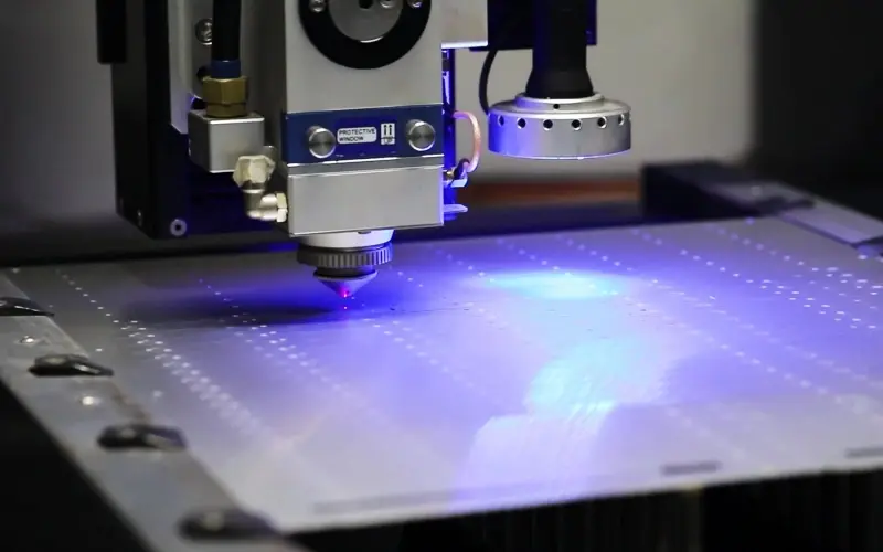
3.10 Laser drilling (LASER DRILLING)
Laser drilling uses laser energy to burn resin and form blind vias. Laser energy decays from top to bottom, so hole diameter narrows with depth. Typical hole size is 4–6 mil (0.10–0.15 mm). According to IPC6016, holes ≤0.15 mm are called micro-vias.
Holes larger than 0.15 mm need spiral drilling. Speed drops and cost rises fast. Mainstream laser tools now use three-shot drilling. Speed is 100–200 holes per second. Smaller holes can be faster (0.100 mm hole ~120 holes/sec; 0.076 mm hole ~170 holes/sec).
3.11 Laser via metallization
Laser holes burn the hole wall and leave char. The second copper layer may oxidize. High-pressure water wash is needed to remove drill residue. Micro-via char is hard to remove. Stacked two-level HDI needs special blind-via plating and copper filling (COPPER FILLING). This is costly and used for high-end products.
3.12 Third inner dry film
After laser via metallization, do a second Conformal mask1. Then return to inner dry film steps to make layers 2 and 7 traces. After traces are done, do black/brown oxidation and a third lamination. Then make the third blind via etch step 1 and the second blind via etch step 2 to prepare for the second laser drilling.
Second-level HDI needs many alignments. Error can add up. This makes scrap rate higher. From easier to harder in via combinations:
1–2 + 2–3 vias < only 1–3 vias < 1–2 + 1–3 vias < 2–3 + 1–3 vias < 1–2 + 2–3 + 1–3 vias.
HDI vias should be designed symmetrically.
3.13 Second laser drilling
Perform the second laser drilling step as planned for two-level HDI. This follows similar rules to the first laser drilling but needs careful alignment and via planning.
3.14 Mechanical drilling (drill through holes)
After laser steps, perform mechanical drilling for through holes. This step drills holes that go through the whole panel.
3.15 Drill residue removal and via plating (P.T.H)
Plate the blind vias and through holes together so all vias are metallized. At this point the special HDI flow ends. From now on, the board follows standard PCB finishing steps.
3.16 Outer-layer dry film and pattern plating (DRY FILM & PATTERN PLATING)
Outer pattern transfer is similar to inner layers. Main difference is the plating method:
- Subtractive method: use negative film. The hardened dry film stays as circuit. Etch and strip the film to keep the circuit.
- Additive/normal method: use positive film. The hardened dry film covers non-circuit areas. Do pattern plating (copper then tin), then strip film, do alkaline etch, remove tin, and keep the circuit.
3.17 Wet-film solder mask (WET FILM SOLDER MASK)
Solder mask coats the board surface. It prevents wrong soldering, moisture or chemicals from causing shorts, and protects traces from physical damage. This keeps PCB function stable.
Process: pre-clean → coat → pre-bake → exposure → develop → UV cure → thermal cure. Key control points: solder mask alignment, mask bridge size, via production, and mask thickness. Ink quality affects later surface finish, SMT mounting, and board life.
3.18 Selective immersion gold (IMMERSION GOLD)
Chemical nickel/gold plating is a surface finish after solder mask. It suits PCBs with small trace pitch and many surface mount parts. It helps pad coplanarity and flatness. Gold is stable and protective. Plating specs: nickel ~5 μm, gold 0.05–0.1 μm. Too thick gold can crack and make weak solder joints. Too thin gold has poor protection. ENIG is less solderable in some cases and may show dark pad defects.
3.19 Legend printing (C/M PRINTING)
Print legends and markings using legend ink. This helps later assembly and service.
3.20 Milling and profiling (PROFILING)
Cut the finished panel to UNIT or SET size with CNC routers. Do edge trimming and slot milling. If V-CUT is needed, add steps accordingly. Key parameters: profile tolerance, chamfer size, inner corner radius. Leave safe distance between patterns and board edge.
3.21 Electrical test (E-TEST)
This is the continuity and isolation test. Main methods are bed-of-nails test and flying probe test:
- Bed-of-nails: generic or custom fixtures. Generic fixtures cost more but suit many PCBs. Custom fixtures are cheaper per part but only for specific PCBs.
- Flying probe: moves probes to test nets. It is flexible and good for many small runs.
3.22 OSP (Organic Solderability Preservative)
OSP forms an organic film on bare copper pads and through holes after electrical test and visual check. Film thickness is 0.3–0.5 μm. Decompose temp about 300 °C.
Main advantages: flat plating that fits small pitch PCBs; simple process, low pollution, low cost, and good solderability. Drawbacks: film is thin and easy to scratch. Shelf life is short.
Today, ENIG + OSP combinations are used for high precision boards. They give protection and solderability and are a lead-free option to replace HASL in some cases. Cost is higher.
3.23 Final audit (FINAL AUDIT)
Inspect PCB appearance, size, electrical performance, and plating quality. Make sure everything meets design and industry standards.
3.24 Packing (PACKING)
Pack passing PCBs to prevent moisture and scratches. Protect boards during shipping and store them well for later use.